Resonant tunneling diode based high-sensitivity detector with low dark current

A resonant tunneling and high-sensitivity technology, applied in circuits, electrical components, semiconductor devices, etc., can solve the problems of limiting the application of resonant tunneling diode detectors, large tunneling current and noise current, and large dark current of devices, achieving The effect of increasing the difficulty of passing, reducing the current density, and increasing the height of the barrier

Active Publication Date: 2015-05-27
INST OF SEMICONDUCTORS - CHINESE ACAD OF SCI
View PDF5 Cites 13 Cited by
  • Summary
  • Abstract
  • Description
  • Claims
  • Application Information

AI Technical Summary

Problems solved by technology

In the nin-type doped structure, because of its low potential barrier and the closeness between the Fermi level and the ground state energy level of the potential well, there are many carriers passing through the double barrier single potential well structure, and the current density is very large, which means The tunneling current and noise current are very large, and the dark current output by the device will be very large.
When we want to perform photoelectric detection, excessive dark curre

Method used


Image

  • Resonant tunneling diode based high-sensitivity detector with low dark current
  • Resonant tunneling diode based high-sensitivity detector with low dark current
  • Resonant tunneling diode based high-sensitivity detector with low dark current

Examples


Embodiment Construction

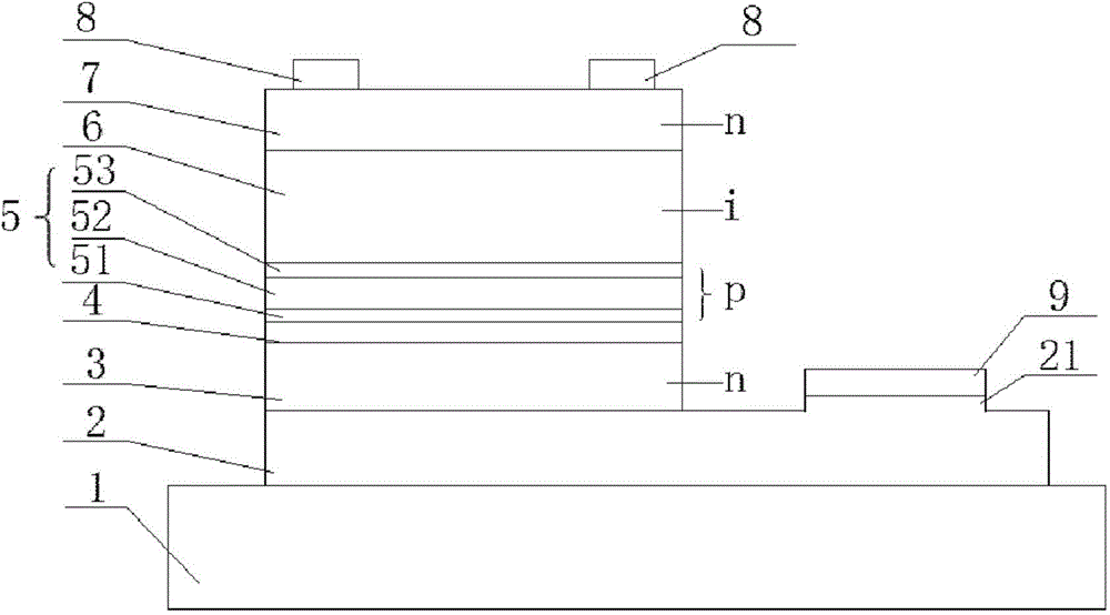
[0025] see figure 1 As shown, the present invention provides a low dark current resonant tunneling diode high-sensitivity detector, including:

[0026] A substrate 1, the material of the substrate 1 is N+ type InP, and its main function is as a substrate for epitaxial layer growth;

[0027] An emitter contact layer 2, which is made on the substrate 1, the material of the emitter contact layer 2 is In 0.53 Ga 0.47 As, the doping concentration is n-type 2×10 18 -5×10 18-3 , with a thickness of 400-600nm, the main function is to form a low-resistance emitter ohmic contact;

[0028] An emitter region 3, which is made on the emitter contact layer 2, a table 21 is formed on the other side of the emitter contact layer 2, and the material of the emitter contact layer is In 0.53 Ga 0.47 As, the doping concentration is n-type 1×10 18 -5×10 18 cm -3 , with a thickness of 200-400nm, the main function is to form the emission region of the resonant tunneling diode, so that the Ferm...


PUM

PropertyMeasurementUnit
Doping concentrationaaaaaaaaaa
Thicknessaaaaaaaaaa
Doping concentrationaaaaaaaaaa

Abstract

A resonant tunneling diode based high-sensitivity detector with low dark current comprises a substrate, an emitting electrode contact layer, an emitting region, an isolating layer, a double-potential-barrier structure, an absorption layer, a collector region, an upper electrode and a lower electrode, wherein the emitting electrode contact layer is manufactured on the substrate; the emitting region is manufactured on the emitting electrode contact layer, and a table board is formed on the other side of the emitting electrode contact layer; the isolating layer is manufactured on the emitting region; the double-potential-barrier structure is manufactured on the isolating layer; the absorption layer is manufactured on the double-potential-barrier structure; the collector region is manufactured on the absorption layer; the upper electrode is manufactured on the collector region; the lower electrode is manufactured on the table board on the other side of the emitting electrode contact layer. According to the resonant tunneling diode based high-sensitivity detector with the low dark current, the dark current can be further reduced; with the adoption of npin type doping, the low dark current can be obtained by the resonant tunneling diode based near-infrared detector.

Description

technical field [0001] The invention relates to a near-infrared detector, in particular to a resonant tunneling diode high-sensitivity detector with low dark current and working at room temperature based on the resonant tunneling effect. Background technique [0002] Resonant tunneling diodes are one of the outstanding representatives of nanoelectronic devices. When nanoelectronic devices are coming, resonant tunneling diodes with the advantages of high frequency, low voltage, negative resistance, and multiple functions with a small number of devices will surely be obtained. More attention and development. Resonant tunneling diode, as the first nanoelectronic device intensively studied, has developed earlier, faster, more mature, and has more application prospects than other nanoelectronic devices. Now it is mainly used in detectors, oscillators, memories And photoelectric switches, etc., is an important symbol of the development of quantum coupling devices and their circui...

Claims


Application Information

Patent Timeline
IPC IPC(8): H01L31/101H01L31/0304
Inventor 裴康明倪海桥詹锋董宇牛智川
Owner INST OF SEMICONDUCTORS - CHINESE ACAD OF SCI
Why Eureka
Try Eureka