Forming method of PMOS (P-channel metal oxide semiconductor) transistor

A transistor and semiconductor technology, applied in semiconductor/solid-state device manufacturing, electrical components, circuits, etc., can solve problems such as low mobility and low saturation current of PMOS transistors, and achieve enhanced mobility, increased mobility, and lattice structure. full effect

Inactive Publication Date: 2015-06-03
SEMICON MFG INT (SHANGHAI) CORP
View PDF3 Cites 5 Cited by
  • Summary
  • Abstract
  • Description
  • Claims
  • Application Information

AI Technical Summary

Problems solved by technology

[0006] In NMOS transistors, the carriers are electrons, and the mobility in silicon is large, so that the NMOS transistor has a high saturation current; while in the PMOS transistor, the carr

Method used


Image

  • Forming method of PMOS (P-channel metal oxide semiconductor) transistor
  • Forming method of PMOS (P-channel metal oxide semiconductor) transistor
  • Forming method of PMOS (P-channel metal oxide semiconductor) transistor

Examples


Embodiment Construction

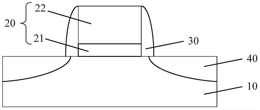
[0034] As mentioned in the background art, the performance of the PMOS transistors formed in the prior art needs to be further improved.

[0035] Studies have found that the mobility of carrier holes in PMOS transistors in silicon germanium is greater than that in silicon. Using silicon germanium materials as the channel material of transistors can improve the hole mobility of PMOS transistors, thereby improving the mobility of PMOS transistors. the saturation current. In one embodiment, a silicon germanium layer may be formed by epitaxy on the substrate, and then the silicon germanium layer may be etched to serve as a channel region of the PMOS transistor. However, the silicon germanium layer formed by the epitaxial process has low yield and high cost, and the silicon germanium layer formed by the epitaxial process has many defects, which will reduce the quality of the channel region of the formed transistor. affect the performance of transistors.

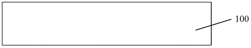
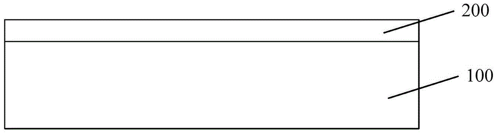
[0036] In one embodiment...


PUM

PropertyMeasurementUnit
Thicknessaaaaaaaaaa

Abstract

The invention provides a forming method of a PMOS (P-channel metal oxide semiconductor) transistor. The method comprises the following steps that a semiconductor substrate is provided; a pseudo grid dielectric material layer and a pseudo grid electrode positioned on the surface of the pseudo grid dielectric layer are formed on the semiconductor substrate, and the pseudo grid electrode covers the partial pseudo grid dielectric material layer; a dielectric layer is formed on the semiconductor substrate, the surface of the dielectric layer is flush with the surface of the pseudo grid electrode, the pseudo grid electrode and a partial pseudo grid dielectric layer positioned under the pseudo grid electrode are removed, and a first groove is formed; the bottom of the first groove is subjected to plasma injection for forming an injection region, and the migration rate of carriers can be enhanced through plasmas; the injection region is subjected to recrystallization processing, and the defects in the injection region are eliminated, so that the injection region can become a channel region; a grid electrode structure is formed in the first groove, and the grid electrode structure comprises a grid dielectric layer positioned at the surface of the inner wall of the first groove and a grid electrode positioned on the surface of the grid dielectric layer. When the method is adopted, the migration rate of the carriers of the PMOS transistor can be improved.

Description

technical field [0001] The invention relates to the technical field of semiconductors, in particular to a method for forming a PMOS transistor. Background technique [0002] MOS transistors are the most basic electronic components in integrated circuits, and the performance of MOS transistors has a huge impact on the performance of the entire chip. [0003] Please refer to figure 1 , is a schematic structural diagram of a MOS transistor in the prior art. [0004] The MOS transistor comprises: a semiconductor substrate 10; a gate structure 20 located on the surface of the semiconductor substrate 10, the gate structure 20 comprising a gate dielectric layer 21 located on the surface of the semiconductor substrate 10 and a gate dielectric layer located on the surface of the semiconductor substrate 10 The gate 22 on the surface of the gate structure 21; the sidewalls 30 on the sidewall surfaces on both sides of the gate structure 20; the source and drain 40 in the semiconductor...

Claims


Application Information

Patent Timeline
IPC IPC(8): H01L21/336
Inventor 三重野文健
Owner SEMICON MFG INT (SHANGHAI) CORP
Why Eureka
Try Eureka