Semiconductor memory device and preparation method thereof

A technology of storage devices and semiconductors, which is applied in semiconductor devices, semiconductor/solid-state device manufacturing, electric solid-state devices, etc., and can solve problems such as high power consumption, reduced coupling rate, and high operating voltage

Inactive Publication Date: 2015-06-03
SEMICON MFG INT (SHANGHAI) CORP
View PDF3 Cites 8 Cited by
  • Summary
  • Abstract
  • Description
  • Claims
  • Application Information

AI Technical Summary

Problems solved by technology

[0005] The floating gate structure prepared in the prior art has a relatively large coupling ratio, among which such as Figure 1d As shown, the tunnel capacitance Ctunnel=Cgs+Cgb+Cgd, the total capacitance of the device Ctotal=Cono+Ctunnel, where Kono=Cono/Ctotal, because the device has a low coupling rat

Method used


Image

  • Semiconductor memory device and preparation method thereof
  • Semiconductor memory device and preparation method thereof
  • Semiconductor memory device and preparation method thereof

Examples


Embodiment 1

[0042] Attached below Figure 2a-2d A specific embodiment of the present invention will be described.

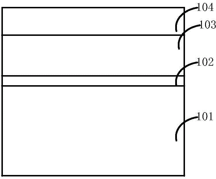
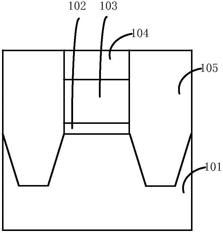
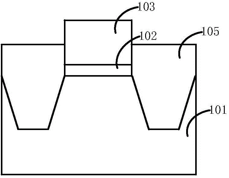
[0043] First, step 201 is performed to provide a semiconductor substrate 201 on which a tunnel oxide layer (tunnel oxide) 202 , a floating gate layer 203 and a mask layer 204 are formed.

[0044] Specifically, please refer to Figure 2a, first provide a semiconductor substrate 201, wherein the semiconductor substrate 201 can be at least one of the materials mentioned below: silicon, silicon-on-insulator (SOI), silicon-on-insulator (SSOI), germanium-on-insulator Silicon-on-insulator (S-SiGeOI), silicon-germanium-on-insulator (SiGeOI), and germanium-on-insulator (GeOI). In addition, an active region may be defined on the semiconductor substrate 201 . Other active devices may also be included on the active area, which are not marked in the shown figures for convenience.

[0045] The semiconductor substrate 201 can be selected as P-type, and a tunnel oxide layer is deposited...

Embodiment 2

[0082] The present invention also provides a floating gate structure, including:

[0083] semiconductor substrate 201;

[0084] a tunnel oxide layer 202 located on the semiconductor substrate;

[0085] The floating gate, located on the tunnel oxide layer 202 , includes a floating gate layer 203 and a hemispherical floating gate film 206 located on the floating gate layer 203 .

[0086] Wherein, the critical dimension of the hemispherical floating gate film 206 is greater than the critical dimension of the floating gate layer 03, the hemispherical floating gate film 206 is concave overall, and its inner surface has hemispherical floating gate crystal grains to increase The surface area of ​​the floating gate structure.

[0087] Further, the floating gate structure also includes:

[0088] ONO material layer, located above the hemispherical floating gate film 206;

[0089] a control gate layer located above the ONO material layer;

[0090] A shallow trench isolation structur...


PUM

PropertyMeasurementUnit
Thicknessaaaaaaaaaa
Thicknessaaaaaaaaaa
Thicknessaaaaaaaaaa

Abstract

The invention relates to a semiconductor memory device and a preparation method thereof. The method comprises the following steps: providing a semiconductor substrate and forming a tunneling oxide layer, a floating gate layer and a mask layer on the semiconductor substrate; patterning the mask layer, the floating gate layer, the tunneling oxide layer and the semiconductor substrate to form shallow trenches in the semiconductor substrate on the two sides of a floating gate laminate while the floating gate laminate is formed; selecting an isolation material to fill the shallow trenches so as to form a shallow trench isolation structure; removing the mask layer to form a groove on the upper side of the floating gate layer; etching back the isolation material on the two sides of the groove to increase the critical size of the groove; depositing a semi-spherical floating gate film at the bottom and on the side wall of the groove with the increased critical size to form a floating gate structure. The floating gate structure comprises a semi-spherical floating gate film, so the surface area of the floating gate structure is increased, the electric capacity formed by the floating gate is increased, and the performance of the device is improved.

Description

technical field [0001] The present invention relates to a semiconductor memory device, in particular, the present invention relates to a semiconductor memory device and a manufacturing method thereof. Background technique [0002] With the rapid development of portable electronic devices (such as mobile phones, digital cameras, MP3 players, and PDAs, etc.), the requirements for data storage are getting higher and higher. Non-volatile memory has become the most important storage component in these devices because of its ability to save data even when power is off. Among them, because flash memory (flash memory) can achieve a high chip storage density, and no new materials are introduced , The manufacturing process is compatible, therefore, it can be more easily and reliably integrated into own digital and analog circuits. [0003] Floating gate structure memory is one of the important flash memory devices, and it is a mainstream memory type that is widely used and generally ...

Claims


Application Information

Patent Timeline
IPC IPC(8): H01L21/8247H01L21/28H01L27/115H01L29/423
Inventor 宋化龙
Owner SEMICON MFG INT (SHANGHAI) CORP
Why Eureka
Try Eureka