Process method for preparing NiCr wear-resistant coating on copper surface

A process method and wear-resistant coating technology, which is applied in the direction of metal material coating process, coating, etc., can solve the problems of high toxicity, cumbersome process, high porosity of coating, etc., and achieve the effect of strong binding force

Active Publication Date: 2015-06-10
CHANGZHOU UNIV
5 Cites 8 Cited by

AI-Extracted Technical Summary

Problems solved by technology

[0004] In order to make up for the deficiencies in the existing electrochrome plating technology, such as cumbersome process, high toxicity, high coating por...

Abstract

The invention relates to the technical field of mental surface processing and especially discloses a process method for preparing a NiCr wear-resistant coating on copper surface. According to the process method, wear-resisting property and corrosion-resisting property of the Cu surface are improved by surface alloying and surface pre-treating processes. The process method mainly comprises the following steps: (1) pre-treating the copper surface; (2) preparing and treating the NiCr deposition electrode; and (3) preparing the wear-resistant Ni/Cr coating. The process method is simple in process, rational in design, convenient to operate and low in processing cost; the process method has easier processes when compared with the vapor depositing and sputtering technologies and is free of problems such as environmental pollutions produced in the plating process. According to the process method, technological parameters are changed in the coating preparation process to obtain coatings of various thicknesses and performances. The NiCr coating prepared by the process method has stronger binding forces to the matrix when compared with coatings prepared by vapor depositing, sputtering and plating technologies. The process method has the characteristics of metallurgical bonding between the coating and the matrix so that good wear-resistant properties can be maintained. Moreover, the coating is compact so that oxidation can be effectively inhibited.

Application Domain

Technology Topic

Image

  • Process method for preparing NiCr wear-resistant coating on copper surface

Examples

  • Experimental program(4)

Example Embodiment

[0026] Example 1:
[0027] 1): Surface pretreatment: 400-1200 for copper samples # After grinding the sandpaper step by step, put the sample in the acetone solution for ultrasonic assisted degreasing and cleaning for 3 minutes, then rinse with deionized water and blow dry for later use.
[0028] 2): Pretreatment of the deposition electrode surface: select pure Ni (purity greater than 99.9wt%, the same in the following examples) and pure Cr (purity greater than 99.9wt%, the same in the following examples) electrode rods (both diameters are 3mm) Put it in acetone solution for ultrasonic assisted degreasing and cleaning for 5 minutes, then rinse with deionized water and blow dry for later use.
[0029] 3): Coating preparation process: use the selected copper sample as the substrate material, as the cathode in the deposition process, connect the cathode of the power supply device, use the Ni rod as the deposition electrode, set the deposition process parameters, and the deposition voltage is 80V. The frequency is 300Hz, the pulse width is 200μs, the duty cycle is 40%, 8L/min argon gas is used as the protective gas, the deposition electrode rotation speed is maintained at 1000r/min, and the deposition time is 4min; when a layer of Ni is formed on the surface of the copper Then, the treated Cr was used as the deposition electrode, and the same process parameters were set. The deposition voltage was 80V, the frequency was 300Hz, the pulse width was 200μs, the duty cycle was 40%, and the rotation speed of the deposition electrode was maintained at 1000r/min. Depositing 4 minutes on the Ni layer, a dense NiCr deposition layer can be prepared on the copper surface. The thickness of the deposition layer is about 5μm, and the mass ratio of Ni/Cr in the coating is about 1:1.
[0030] figure 1 Is the XRD pattern of the deposited layer of Example 1, figure 1 It is to explain that Cr and Ni coatings can be prepared on the copper surface through this process, and the coating preparation effect is good. In addition, the appearance of NiCu alloy in the coating also further illustrates that the Ni deposited on the surface of the substrate and the NiCu formed by mutual fusion of the substrate Alloy, this is also a metallurgical bond formed. Because of the metallurgical bond formed by the coating, it has a good bond strength. This is also consistent with the high-energy micro-arc spark deposition technology, and the bond strength is high.

Example Embodiment

[0031] Example 2:
[0032] 1): Surface pretreatment: use 400-1200 pure copper flake samples of 2mm*2mm respectively # The sandpaper is polished step by step, the sample is placed in an acetone solution for ultrasonic assisted degreasing and cleaning for 5 minutes, and then rinsed with deionized water to dry for use.
[0033] 2): Pretreatment of the deposition electrode surface: select pure Ni (purity greater than 99.9wt%, the same in the following examples) and pure Cr (purity greater than 99.9wt%, the same in the following examples) electrode rods (both diameters are 2mm) Put it in acetone solution for ultrasonic assisted degreasing and cleaning for 5 minutes, then rinse with deionized water and blow dry for later use.
[0034] 3): Coating preparation process: select the copper sample as the base material, use it as the cathode during the deposition process, connect the cathode of the power supply device, use the Ni rod as the deposition electrode, set the deposition process parameters, the deposition voltage is 90V, and the frequency is 400Hz, pulse width of 250μs, duty cycle of 50%, 10L/min of argon gas is used as the protective gas, the rotation speed of the deposition electrode is maintained at 3000r/min, and the deposition time is 5min; when a layer of Ni is formed on the copper surface, Use the processed Cr rod as the deposition electrode, set the same process parameters, the deposition voltage is 90V, the frequency is 400Hz, the pulse width is 250μs, the duty cycle is 50%, and the rotation speed of the deposition electrode is maintained at 3000r/min. The time for depositing Cr on the Ni layer is 2 minutes, and a dense deposition layer can be prepared on the copper surface. The thickness of the deposition layer is about 10 μm, and the adhesion is good. The mass ratio of NiCr formed after the deposition process is about 5:2.
[0035] The XRD pattern of the deposited layer of Example 2 is similar to that of Example 1.

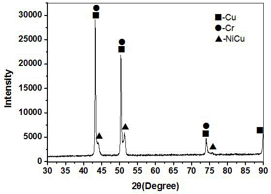
Example Embodiment

[0036] Example 3:
[0037] 1): Surface pretreatment: use 400-1200 for pure copper samples respectively # The sandpaper is polished step by step, the sample is placed in an acetone solution for ultrasonic assisted degreasing and cleaning for 5 minutes, and then rinsed with deionized water to dry for use.
[0038] 2): Pretreatment of the deposition electrode surface: select pure Ni (purity greater than 99.9wt%, the same in the following examples) and pure Cr (purity greater than 99.9wt%, the same in the following examples) electrode rods (both diameters are 3mm) Put it in acetone solution for ultrasonic assisted degreasing and cleaning for 5 minutes, then rinse with deionized water and blow dry for later use.
[0039] 3): Coating preparation process: use the selected copper sample as the substrate material, as the cathode in the deposition process, connect the cathode of the power supply device, use the Ni rod as the deposition electrode, set the deposition process parameters, and the deposition voltage is 80V. The frequency is 400Hz, the pulse width is 200μs, the duty cycle is 45%, 10L/min of argon is used as the protective gas, the deposition electrode rotation speed is maintained at 4000r/min, and the deposition time is 4min; when a layer of Ni is formed on the copper surface After that, the treated Cr rod was used as the deposition electrode, and the same process parameters were set. The deposition voltage was 80V, the frequency was 400Hz, the pulse width was 200μs, the duty cycle was 45%, and the rotation speed of the deposition electrode was maintained at 4000r/min. Depositing on the formed Ni layer for 2 minutes, a dense deposition layer can be prepared on the copper surface. The thickness of the deposition layer is about 7 μm, and the mass ratio of the formed NiCr is about 2:1.
[0040] The XRD pattern of the deposited layer of Example 3 is similar to that of Example 1.

PUM

PropertyMeasurementUnit
Thickness5.0µm
Thickness10.0µm
Thickness7.0µm
tensileMPa
Particle sizePa
strength10

Description & Claims & Application Information

We can also present the details of the Description, Claims and Application information to help users get a comprehensive understanding of the technical details of the patent, such as background art, summary of invention, brief description of drawings, description of embodiments, and other original content. On the other hand, users can also determine the specific scope of protection of the technology through the list of claims; as well as understand the changes in the life cycle of the technology with the presentation of the patent timeline. Login to view more.

Similar technology patents

Classification and recommendation of technical efficacy words

Why Eureka
Try Eureka