Transistor forming method

A transistor and dry cleaning technology, which is applied in the direction of semiconductor devices, semiconductor/solid-state device manufacturing, electrical components, etc., can solve the problem of unclean removal of dummy gate 02, etc., and achieve the effect of improving etching effect, good effect, and avoiding pollution

Active Publication Date: 2015-06-10
SEMICON MFG INT (SHANGHAI) CORP
View PDF5 Cites 3 Cited by
  • Summary
  • Abstract
  • Description
  • Claims
  • Application Information

AI Technical Summary

Problems solved by technology

The dummy gate 02 is usually formed of polysilicon. In the prior art, a combination of anisotropic dry etching and wet etching is generally used to remove the dummy gate 02 made of polysilicon. However, in the prior art, ...

Method used


Image

  • Transistor forming method
  • Transistor forming method
  • Transistor forming method

Examples


Embodiment Construction

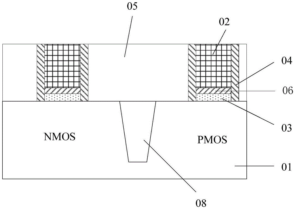
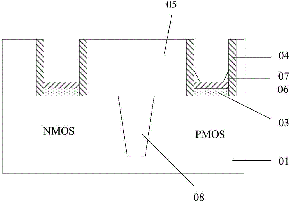
[0034] After dry etching removes most of the dummy gates in the dummy gate structure, pollutants such as particles and organic matter will be produced on the surface of the remaining dummy gates, and polymer particles and oxide layers, etc., will seriously affect the subsequent process. Particles and oxide layer adhere to the surface of the residual dummy gate. Due to the strong selectivity of the subsequent wet etching, the residual dummy gate blocked by polymer particles and oxide layer is difficult to be etched clean, and it is easy to make the final formed Transistors develop defects.

[0035] In order to wet-etch the pseudo-gate dielectric layer with pseudo-gate residues and other pollutants on the surface, the concentration of the etching solution used is high, and the high-concentration etching solution is easy to corrode the interlayer dielectric layer.

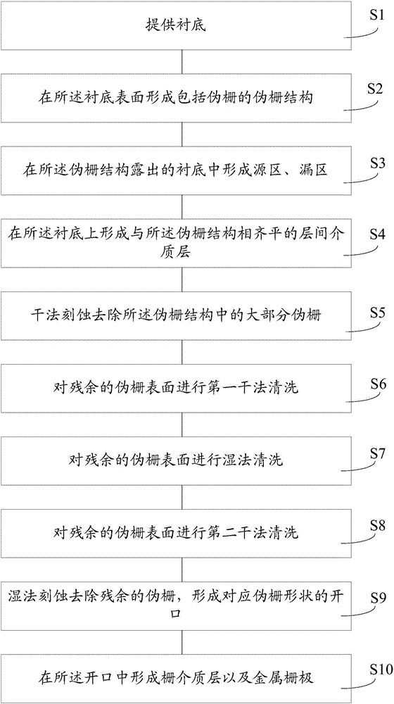
[0036] In order to solve the above technical problems, the present invention provides a method for forming a transi...


PUM


Abstract

The invention provides a transistor forming method. The method includes providing a substrate; forming a false grid structure comprising a false grid on the surface of the substrate; forming a source region and a leak region on the substrate exposed in the false grid structure; forming an interlayer medium layer aligned with the false grid structure on the substrate; removing majority of the false grid of the false grid structure by dry etching; performing first dry washing on the surface of the remained false grid; performing wet washing on the surface of the remained false grid; performing second dry washing on the surface of the remained false grid; removing the remained false grid by wet etching, and forming an opening corresponding to the false grid in the shape; forming a grid medium layer and a metal grid electrode in the opening. By means of the first dry washing, the wet washing and the second dry washing, the contaminant remained on the surface of the false grid is removed after the false grid is formed by dry etching, and the performance of a transistor is optimized.

Description

technical field [0001] The present invention relates to the field of semiconductors, in particular to a method for forming a transistor. Background technique [0002] In the high-K dielectric / metal gate engineering of transistors, after high-temperature annealing for ion activation, dummy gates such as polysilicon gates need to be removed, and then filled with metal gate electrodes to form a high-K dielectric / metal gate structure. [0003] refer to figure 1 and figure 2 , shows a method for forming a transistor in the prior art. Such as figure 1 As shown, the shallow trench isolation region 08 is formed in the substrate 01, the dummy gate structure of the NMOS transistor is formed on the left side of the shallow trench isolation region 08, and the dummy gate structure of the PMOS transistor is formed on the right side, and each dummy gate structure Including a gate dielectric layer 03, a capping layer 06, and a dummy gate 02, the sidewall of the dummy gate structure is ...

Claims


Application Information

Patent Timeline
IPC IPC(8): H01L21/336H01L21/28
Inventor 曾以志赵杰宋伟基
Owner SEMICON MFG INT (SHANGHAI) CORP
Why Eureka
Try Eureka