Supercharge Your Innovation With Domain-Expert AI Agents!

Method for collaboratively and optimally designing high-speed IC-QFN (integrated circuit-quad flat no-lead) packages

A high-speed, packaged structure technology, applied in semiconductor/solid-state device components, semiconductor devices, electrical components, etc., can solve problems such as physical stress cannot be eliminated

Inactive Publication Date: 2015-06-10
SHANGHAI RES INST OF MICROELECTRONICS SHRIME PEKING UNIV
View PDF4 Cites 4 Cited by
  • Summary
  • Abstract
  • Description
  • Claims
  • Application Information

AI Technical Summary

Problems solved by technology

The electroplating annealing in step o can be used to reduce thermal stress. However, due to the different environment of high temperature curing and electroplating annealing, high temperature curing will inevitably introduce some physical stress that cannot be eliminated.

Method used


Image

  • Method for collaboratively and optimally designing high-speed IC-QFN (integrated circuit-quad flat no-lead) packages
  • Method for collaboratively and optimally designing high-speed IC-QFN (integrated circuit-quad flat no-lead) packages
  • Method for collaboratively and optimally designing high-speed IC-QFN (integrated circuit-quad flat no-lead) packages

Examples


Embodiment Construction

[0021] The high-speed IC-QFN package of the present invention will be further described in detail below in conjunction with the accompanying drawings.

[0022] Firstly, the specific implementation manner of the QFN package described in the present invention is introduced. QFN has excellent high-frequency characteristics. If the price advantage of QFN can be maintained, the three-dimensional packaging of QFN will have a wider range of applications.

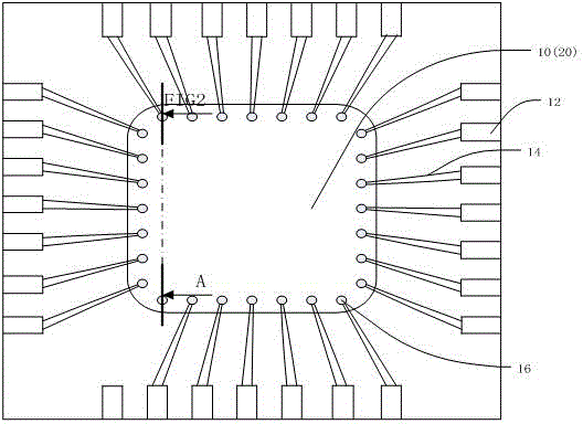
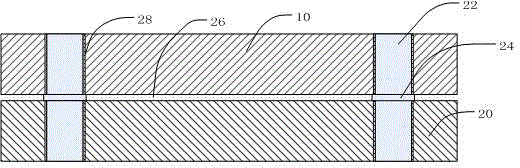
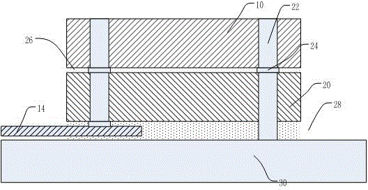
[0023] Such as figure 1 Shown is a schematic diagram of a top view of a QFN three-dimensional package, 10 and 20 are a high-speed IC chip and a control chip respectively, and the two are connected through TSV technology. The bumps of the three-dimensional package and the QFN pads are connected by QFN wiring. Compared with traditional bonding wire gold wires, less parasitics will be introduced and the cost will be reduced.

[0024] For high-speed ICs, any effort to reduce the path to ground will optimize high-frequency performance...


PUM


Abstract

The invention discloses a method for collaboratively and optimally designing high-speed IC-QFN (integrated circuit-quad flat no-lead) packages. The method has the advantages that each package structure designed by the aid of the method comprises a high-speed IC chip and relevant control chips, each high-speed IC chip is connected with the corresponding relevant control chips by through-silicon-vias (TSV), and accordingly parasitic effects of leads of RF (radiofrequency) chips can be reduced by the aid of three-dimensional package technologies; bonding pads with exposed centers are packaged for the QFN packages, so that residual heat can be effectively absorbed, and heat stress on bottom chips of three-dimensional packages can be effectively improved; three-dimensional subpackages are mainly applied to ball grid array packages under the consideration of the quantities of pins of the chips, and the performance of high-speed ICs can be greatly optimized if the QFN packages can be used in the three-dimensional packages with few pins owing to the low QFN cost and mature QFN package processes; heat stress generated in package procedures increasingly becomes an important factor which can affect the performance of the chips for the three-dimensional packages with high integration levels, the method for collaboratively and optimally designing the QFN packages is based on generation of the heat stress on chip packages and analysis on parasitism of the high-speed ICs, and the QFN packages are optimized from the aspects of reducing the parasitism and reducing the heat stress.

Description

technical field [0001] The invention relates to the field of integrated circuit packaging, in particular to a method for optimizing high-speed ICs. Background technique [0002] In the semiconductor packaging process, Quad Flat No-lead Package (QFN) has many advantages, such as good heat dissipation characteristics, low packaging cost, relatively mature technology, and excellent electrical performance, etc. This enables QFN packaging to be used in RF circuits. However, due to the technology and cost of three-dimensional packaging, as well as the limitation of QFN pins, three-dimensional packaging technology is mainly used in the packaging form of BGA, and many complex chips still cannot use QFN packaging when three-dimensional packaging is required. The invention adopts QFN three-dimensional packaging for the chip under the condition of low number of pins, which greatly reduces the parasitic caused by chip interconnection. [0003] With the improvement of the integration l...

Claims


Application Information

Patent Timeline
Patent Type & Authority Applications(China)
IPC IPC(8): H01L23/522H01L23/48H01L23/488
CPCH01L2224/16145
Inventor 刘少龙程玉华
Owner SHANGHAI RES INST OF MICROELECTRONICS SHRIME PEKING UNIV
Features
  • R&D
  • Intellectual Property
  • Life Sciences
  • Materials
  • Tech Scout
  • Unparalleled Data Quality
  • Higher Quality Content
  • 60% Fewer Hallucinations
Learn More