Eureka AIR delivers breakthrough ideas for toughest innovation challenges, trusted by R&D personnel around the world.

Preparation process of superconductive Josephson junction covered by edge of in-situ three-layer film

A technology of edge coverage and preparation process, applied in the field of semiconductor, can solve the problems of increasing process steps, unstable oxide layer, unfavorable integration scale of patterns, etc., and achieves the effect of high quality and simple steps

Active Publication Date: 2015-06-10
TSINGHUA UNIV
View PDF2 Cites 26 Cited by
  • Summary
  • Abstract
  • Description
  • Claims
  • Application Information

AI Technical Summary

Problems solved by technology

However, the Josephson junctions prepared by several existing processes have shortcomings in large-scale quantum computing, and it is difficult to meet the conditions of high quality and scalability at the same time.
1) In the standard Nb Josephson junction preparation process, the dissipation of the silicon dioxide insulating layer significantly affects the decoherence time of the device, and the unstable oxide layer of the Nb material itself also weakens its competitiveness relative to the Al material; 2) Al Josephson junctions prepared by double-angle evaporation are of high quality, but redundant patterns are not conducive to the improvement of integration and scale; 3) Al Josephson junctions prepared by other planar processes inevitably require the introduction of insulating layers, which It not only increases the process steps, but also introduces factors that may affect the decoherence of the device

Method used


Image

  • Preparation process of superconductive Josephson junction covered by edge of in-situ three-layer film
  • Preparation process of superconductive Josephson junction covered by edge of in-situ three-layer film
  • Preparation process of superconductive Josephson junction covered by edge of in-situ three-layer film

Examples


Embodiment Construction

[0029] The implementation of the present invention will be described in detail below in conjunction with the drawings and examples.

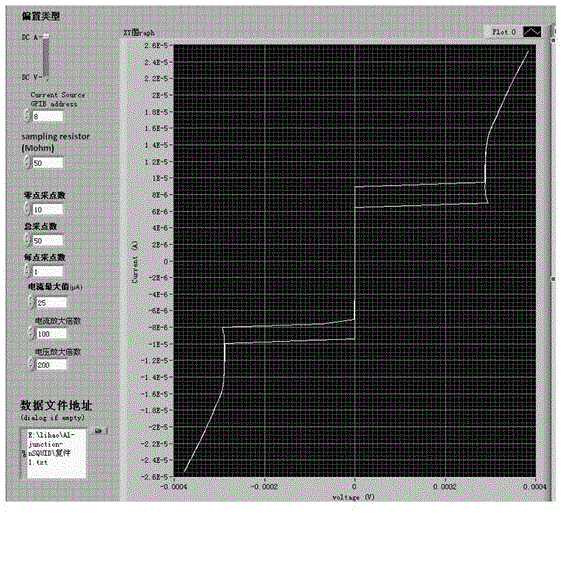
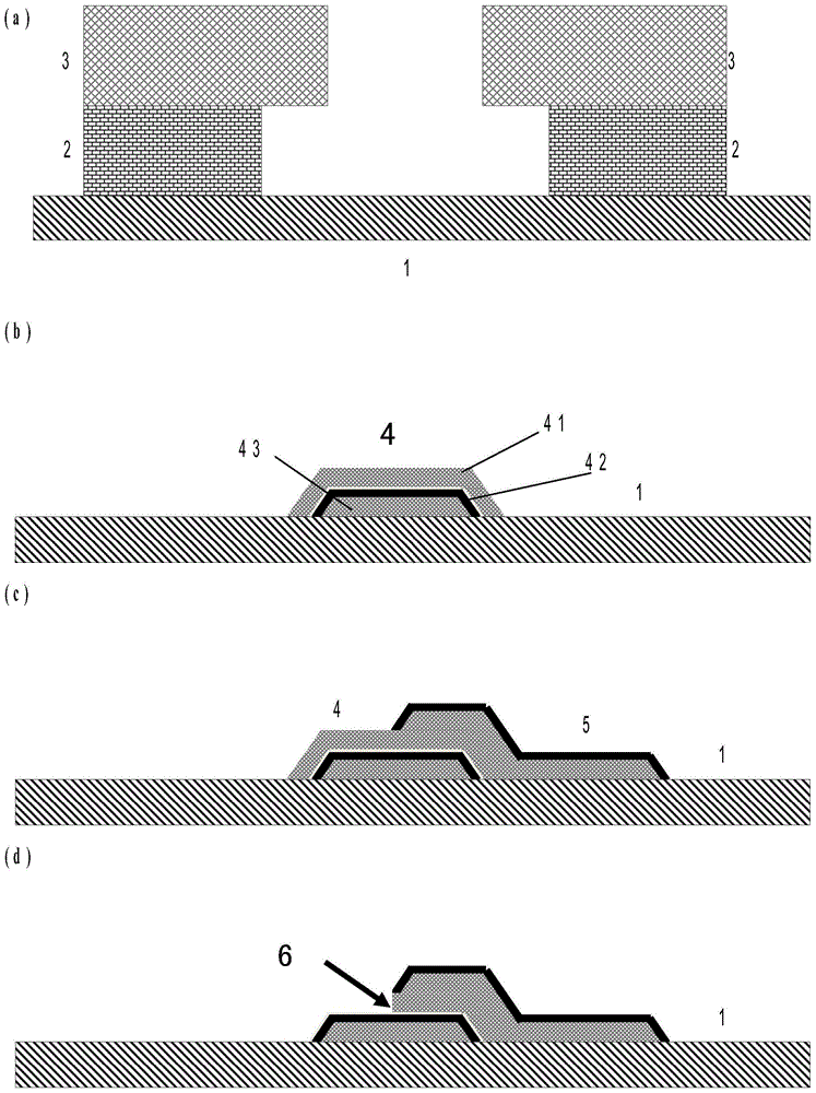
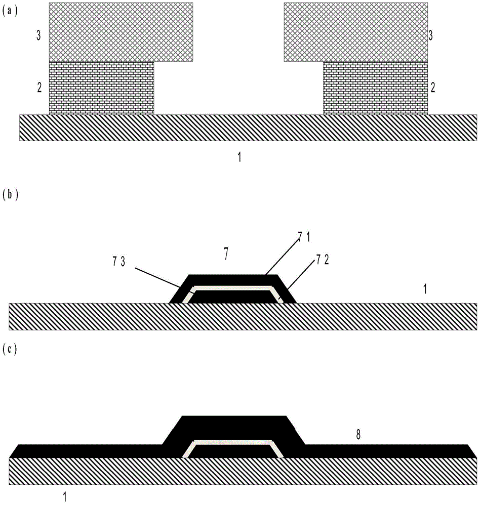
[0030] The invention describes a process for preparing a Josephson junction based on a microelectronic planar process, and its basic process flow consists of three parts: in-situ growth of three layers of film, growth of a lead layer, photolithography and etching to define a junction region. It differs in specific steps and details for Nb Josephson junction and Al Josephson junction. Their preparation procedures are as follows figure 1 and figure 2 shown.

[0031] Nb Josephson junction preparation process:

[0032] (1) Carry out double-layer glue photolithography on sapphire or the silicon chip substrate 1 that surface is thermally oxidized, be respectively upper layer photoresist 3 and lower layer photoresist 2, form good undercut, as figure 1 (a) shown. The process conditions of different photolithography process lines are different. A ...


PUM

PropertyMeasurementUnit
Thicknessaaaaaaaaaa

Abstract

The invention discloses a preparation process of a superconductive Josephson junction covered by the edge of an in-situ three-layer film. A process flow consists of three parts including an in-situ growth three-layer film, a growing wire layer, and a photo-etching and etching defined junction area, wherein the specific steps and details of an Nb (Niobium) Josephson junction and an Al (Aluminum) Josephson junction are different, and finally the Nb Josephson junction without the protection of silicon dioxide and Al or the Al Josephson junction without surplus electrodes or surplus insulating layers can be obtained. The preparation process provided by the invention has the characteristics of being simple in structure, high in quality, large-scale to produce and the like.

Description

technical field [0001] The invention belongs to the technical field of semiconductors, in particular to an in-situ three-layer film edge-covered superconducting Josephson junction preparation process. Background technique [0002] In recent years, superconducting electronics technology has a wide range of demands and applications in the fields of quantum computing, high-performance digital integrated circuits, highly sensitive magnetic field detection, precision physical quantity calibration, and microwave radiation detection. The superconducting Josephson junction is the most basic device in superconducting electronics technology, so the preparation of high-quality Josephson junctions has always attracted people's attention. In particular, the characteristics of nonlinear inductance and scalability make superconducting Josephson junctions the most competitive candidate "artificial atoms" in the field of quantum computing. However, the Josephson junctions prepared by severa...

Claims


Application Information

Patent Timeline
IPC IPC(8): H01L39/24
Inventor 李浩刘其春刘建设李铁夫陈炜
Owner TSINGHUA UNIV
Why Eureka
Eureka Blog
Learn More