
Wide-strip-shaped semiconductor laser cavity mode selecting method

A semiconductor and laser technology, applied in the laser field, can solve the problems of increasing the instability of the waveguide structure, the beam divergence angle, and the beam quality deterioration, and achieve the effect of improving the beam quality.

Inactive Publication Date: 2015-06-10
CHANGCHUN UNIV OF SCI & TECH
View PDF3 Cites 3 Cited by
  • Summary
  • Abstract
  • Description
  • Claims
  • Application Information

AI Technical Summary

Problems solved by technology

Usually, the wide-strip high-power semiconductor laser chip is flip-chip-bonded on a transitional heat sink with high thermal conductivity. Since the large operating current is concentrated in the light-emitting waveguide area, the waste heat generated by the non-radiative recombination of carriers leads to the temperature distribution in the waveguide area as follows: Convex distribution, so that the effective refractive index of the light-emitting waveguide area also presents a convex distribution, which increases the instability of the waveguide structure and the beam divergence angle when the laser is working.
Usually, it is mainly through improving the epitaxial growth quality of laser materials, reducing defects in the light-emitting waveguide region, and suppressing the convex refractive index distribution caused by waste heat. Due to the limitations of the laser structure epitaxial growth source material and the purity of the atmosphere, there are still certain material defects that lead to wide The beam quality of the bar-shaped high-power semiconductor laser is obviously deteriorated under the high-current working condition

Method used


Image

  • Wide-strip-shaped semiconductor laser cavity mode selecting method

Examples


Embodiment Construction

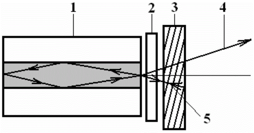
[0006] as attached figure 1 As shown, the rear cavity surface of the wide-strip high-power semiconductor laser chip 1 is coated with a high-reflection film, and the front cavity surface is coated with an anti-reflection film, so that the free-working laser works at a high threshold state. Then, an aspheric cylindrical lens is used to collimate the output beam in the direction of the fast axis, and the beam in the direction of the slow axis remains free to emerge. Then, on the optical axis of the output light beam, place a volume grating 3 whose grating plane normal is inclined to the surface close to the fast axis collimating cylindrical lens 2, whose reflection wavelength is located at the gain spectrum center of the wide strip high-power semiconductor laser chip 1 , to provide efficient spectral feedback. The volume grating 3 is designed for narrow spectrum and narrow angle reflection, and the volume grating feedback beam 5 is fed back to the light-emitting area of ​​the wi...


PUM


Abstract

The invention relates to a wide-strip-shaped semiconductor laser cavity mode selecting method, belongs to the technical field of laser and aims to solve the problem that the beam quality of a wide-strip-shaped large-power semiconductor laser cannot be effectively improved and the application of the wide-strip-shaped large-power semiconductor laser is limited in the prior art. The method is characterized in that a volume grating outer cavity method is used, the inner cavity transverse mode of a wide-strip-shaped large-power semiconductor laser chip which is subjected to fast axis collimation is selected through the narrow-angle beam feedback of the high-reflection volume grating of grating plane normal inclination, and an annular mode in double-peak far field distribution is allowed to receive effective outer cavity feedback; due to the fact that one of the far field peaks is limited by the high-reflection output of the volume grating, single-peak far field lasing is achieved, and the beam quality of the wide-strip-shaped large-power semiconductor laser is improved. The method is applicable to the manufacturing of various wide-strip-shaped large-power semiconductor lasers.

Description

technical field [0001] The invention relates to a cavity mode selection method of a wide-strip semiconductor laser, belonging to the technical field of lasers. Background technique [0002] Wide-strip high-power semiconductor lasers have the advantages of high output power, simple thermal management, and simple power combination. Usually, the wide-strip high-power semiconductor laser chip is flip-chip-bonded on a transitional heat sink with high thermal conductivity. Since the large operating current is concentrated in the light-emitting waveguide area, the waste heat generated by the non-radiative recombination of carriers leads to the temperature distribution in the waveguide area as follows: The convex distribution makes the effective refractive index of the light-emitting waveguide region also present a convex distribution, which increases the instability of the waveguide structure and the beam divergence angle when the laser is working. Usually, it is mainly through im...

Claims


Application Information

Patent Timeline
IPC IPC(8): H01S5/065
Inventor 高欣薄报学乔忠良张晶李辉李特曲轶
Owner CHANGCHUN UNIV OF SCI & TECH
Learn More