Active Coupled Inductor Network Boost Converter

A technology of step-up converter and coupled inductor, which is applied in the direction of adjusting electrical variables, converting DC power input to DC power output, and instruments, etc. It can solve the problems of low voltage stress of the main power switch tube, large number of conversion devices, and low conversion efficiency, etc. problem, to achieve the effect of less number of devices, small size and high conversion efficiency

Active Publication Date: 2017-03-29
HARBIN INST OF TECH
View PDF6 Cites 0 Cited by
  • Summary
  • Abstract
  • Description
  • Claims
  • Application Information

AI Technical Summary

Problems solved by technology

[0003] The present invention aims to solve the problems that existing boost converters adopting a coupled inductor active network structure have a large number of conversion devices, a small boost multiple, low conversion efficiency, high power density, and low voltage stress of the main power switch tube.

Method used


Image

  • Active Coupled Inductor Network Boost Converter
  • Active Coupled Inductor Network Boost Converter
  • Active Coupled Inductor Network Boost Converter

Examples


specific Embodiment approach 1

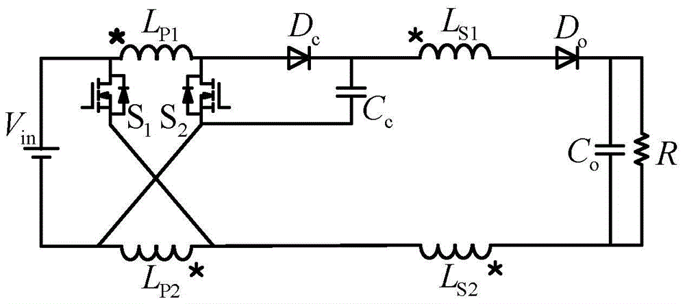
[0019] Specific implementation mode one: refer to figure 1 This embodiment is specifically described. The active coupled inductor network boost converter described in this embodiment includes an X-type active coupled inductor network, a passive lossless clamping circuit, and a filter capacitor C o , rectifier diode D o and resistor R,

[0020] The X-type active coupled inductor network consists of a DC voltage source V in , The primary side of the first coupled inductor L P1 , The secondary side of the first coupled inductor L S1 , The primary side of the second coupled inductor L P2 , The secondary side of the second coupled inductor L S2 , the first power switch tube S 1 and the second power switch S 2 ,

[0021] The passive lossless clamping circuit consists of a clamping diode D c and clamp capacitor C c ,

[0022] The DC voltage source V in The anode of is connected to the first power switch tube S at the same time 1 The anode and primary side of the first c...

specific Embodiment approach 2

[0023] Specific embodiment 2: This embodiment is a further description of the active coupled inductor network boost converter described in specific embodiment 1. In this embodiment, the first power switch tube S 1and the second power switch S 2 Both are MOS tubes or IGBT tubes.

specific Embodiment approach 3

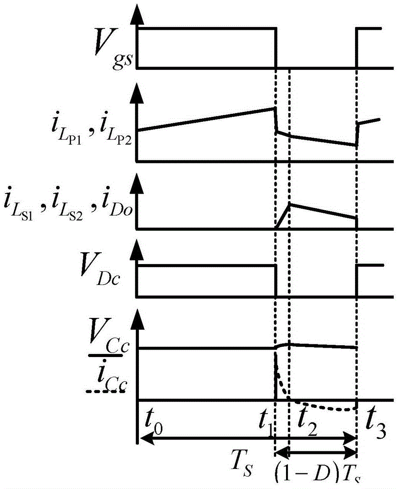
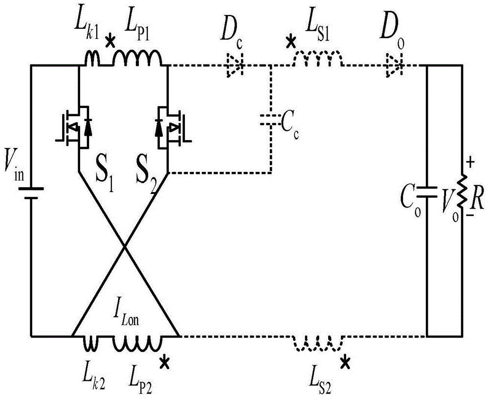
[0024] Specific implementation mode three: refer to Figure 2 to Figure 5 Describe this embodiment in detail. This embodiment is a further description of the active coupled inductor network boost converter described in Embodiment 1. In this embodiment, the working modes of the first coupled inductor and the second coupled inductor are the same , the first coupled inductor and the second coupled inductor are integrated on one magnetic core.

[0025] Operating principle and working process of the present invention are as follows:

[0026] The active coupled inductance network boost converter of the present invention controls the signal voltage V gs ;The primary current of the first coupled inductor and the second coupled inductor primary current First coupled inductor secondary current Secondary coupled inductor current and the output diode current i Do ; Clamp diode voltage V Dc ; Clamp capacitor voltage V Cc and current i Cc The waveform is as figure 2 As shown,...


PUM


Abstract

The invention provides an active coupling inductance network boost converter, and relates to the field of power electronic converters. The active coupling inductance network boost converter solves the problems that according to an existing boost converter of an active coupling inductance network structure, the number of conversion devices is large, the boost multiple is small, the conversion efficiency is low, the power density is large, and the voltage stress of a main power switch tube is low. According to the active coupling inductance network boost converter, the input end of an X-type active coupling inductance network is connected with a direct current voltage source, the output end of the X-type active coupling inductance network is connected with diodes and smoothing capacitors, and a passive lossless clamping circuit is inserted into the X-type active coupling inductance network. The active coupling inductance network boost converter can be applied to occasions of new energy power generation, fuel cells and the like.

Description

technical field [0001] The invention relates to an active coupled inductor network boost converter. It belongs to the field of power electronic converters. Background technique [0002] Boost converters are widely used in industrial fields, such as new energy power generation, fuel cells and other occasions. The traditional boost converter topology is a boost circuit, and the boost circuit is often used in occasions where the input voltage is relatively low and the output voltage is relatively high, such as a single photovoltaic cell module. The commonly used photovoltaic grid-connected structure is to connect multiple photovoltaic cell modules in series and parallel, and then connect the entire photovoltaic array to the grid. However, in actual operation, since photovoltaic cells work outdoors for a long time, they will inevitably be contaminated with dirt such as dust, and will also be blocked by trees, buildings, etc., forming partial shadows, making the working charact...

Claims


Application Information

Patent Timeline
Patent Type & Authority Patents(China)
IPC IPC(8): H02M3/335
CPCH02M3/33561H02M3/33569
Inventor 刘洪臣李飞
Owner HARBIN INST OF TECH
Why Eureka
Try Eureka