Method for reducing density of micro-pinholes in monocrystalline Czochralski silicon

A technology of Czochralski single crystal silicon and micropores, which is applied in the direction of single crystal growth, single crystal growth, chemical instruments and methods, etc., can solve the problems of increasing stabilization time, reducing equipment production efficiency, and high incidence of void-type defects, achieving The effect of reducing Pit and reducing the density of micropores

Active Publication Date: 2015-06-17
GRINM SEMICONDUCTOR MATERIALS CO LTD
View PDF11 Cites 4 Cited by
  • Summary
  • Abstract
  • Description
  • Claims
  • Application Information

AI Technical Summary

Problems solved by technology

Because the silicon melt has a certain viscosity, even by increasing the stabilization time and reducing the production efficiency of the equipment, the incidence of LLPD / Pit-scale void-type defects formed by bubbles with smaller diameters is also higher.

Method used


Image

  • Method for reducing density of micro-pinholes in monocrystalline Czochralski silicon
  • Method for reducing density of micro-pinholes in monocrystalline Czochralski silicon
  • Method for reducing density of micro-pinholes in monocrystalline Czochralski silicon

Examples


Embodiment 1

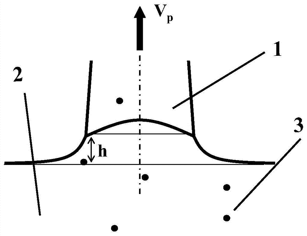
[0028] In a standard Czochralski single crystal furnace, a 22-inch quartz crucible is used to load 110kg of polysilicon; the argon flow rate in the melting stage is 100 slpm, the furnace chamber pressure is 2000 Pa; the stabilization time is 60 minutes, and the rotation speed of the crucible is 1 r / min during the stabilization process.

[0029] Under the conditions of crystal rotation 12r / min, crucible rotation 8r / min, argon gas flow rate 80slpm, furnace chamber pressure 2000Pa, the Vp casting speed is 0.40~1.2mm / min; the average casting speed is 0.80mm / min to grow a diameter of 200mm, etc. A silicon single crystal with a diameter length of about 1060 mm. The crystal was subjected to processing procedures such as slicing, grinding, etching, polishing (CMP), cleaning, etc., and the number and proportion of cavity-type defect silicon wafers in the slicing, etching, and polishing inspection procedures of the branched crystal were counted, as shown in Table 2.

Embodiment 2

[0031] In a standard Czochralski single crystal furnace, a 22-inch quartz crucible is used to load 110kg of polysilicon; the argon flow rate in the melting stage is 40slpm, the furnace chamber pressure is 800Pa; the stabilization time is 120min, and the rotation speed of the crucible during the stabilization process is 1r / min to 8r / min .

[0032] Under the conditions of crystal rotation 12r / min, crucible rotation 8r / min, argon gas flow rate 80slpm, furnace chamber pressure 2000Pa, the Vp casting speed is 0.40~1.2mm / min; the average casting speed is 0.80mm / min to grow a diameter of 200mm, etc. Silicon single crystal with a diameter length of about 1050mm. The crystal is subjected to processing procedures such as slicing, grinding, etching, polishing (CMP), and cleaning. See Table 2 for statistics on the number and proportion of cavity-type defect silicon wafers occurring in the slicing, etching, and polishing inspection processes of the branched crystal.

Embodiment 3

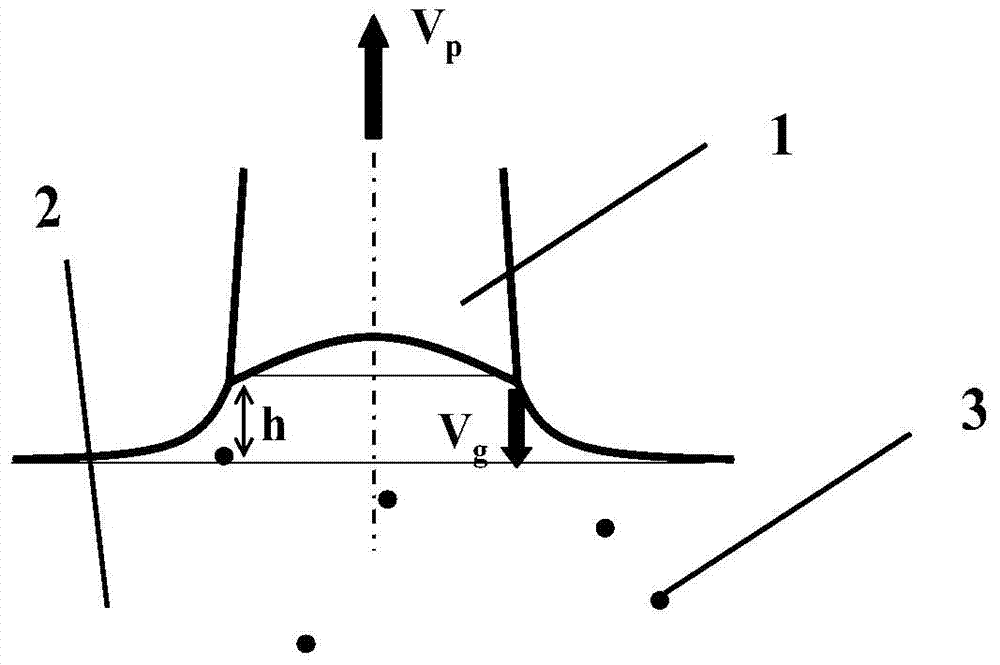
[0034] In a standard Czochralski single crystal furnace, a 22-inch quartz crucible is used to load 110kg of polysilicon; the argon flow rate in the melting stage is 40slpm, the furnace chamber pressure is 800Pa; the stabilization time is 120min, and the rotation speed of the crucible during the stabilization process is 1r / min to 8r / min .

[0035] Under the conditions of crystal rotation 12r / min, crucible rotation 8r / min, argon gas flow rate 80slpm, furnace chamber pressure 2000Pa, the technical solution of the present invention is implemented in the isometric growth process, except that the upward pulling speed Vp=0.40~1.2mm / min; In addition, there is a periodic downward falling speed Vg=0.32~0.96mm / min, the cycle of oscillation operation is 12 seconds, and the frequency of oscillation operation is 1 / 11; the average pulling speed is 0.76mm / min to grow a diameter of 200mm, equal diameter A silicon single crystal with a length of about 1070mm. The crystal is subjected to proces...


PUM

PropertyMeasurementUnit
diameteraaaaaaaaaa

Abstract

The invention provides a method for reducing a density of micro-pinholes in monocrystalline Czochralski silicon. During a process of monocrystalline silicon growth by using the Czochralski method, crystal seeds soaked in a silicon melt is subjected to periodic oscillation operation when pulled up at a front edge of crystallization. The oscillation operation comprises a vertical upward pull process and a vertical downward falling process, wherein the speed Vp of the vertical upward pull process is larger than the speed Vg of the vertical downward falling process. According to the invention and based on a principle of formation of a hole-type defect, periodic oscillation force is generated at the front edge of crystallization, so that periodic oscillation is generated in parts of the melt; micro-pinholes are prevented against adjoining the front edge of crystallization; and micro-pinholes are prevented from entering the inside of silicon crystal. The method is applied to a whole production process of a monocrystalline silicon bar; the density of micro-pinholes in the monocrystalline Czochralski silicon is effectively reduced; and surface defects such as Pit and LLPD of polished wafers are decreased.

Description

technical field [0001] The invention relates to a method for reducing micropore density inside Czochralski single crystal silicon. Background technique [0002] Monocrystalline silicon is the initial material for making integrated circuits. The typical method for producing monocrystalline silicon is the Czochralski method (ie, the CZ process), also known as the Czochralski method. First, the polysilicon raw material is melted in a quartz crucible, protected by flowing argon. After the polysilicon has completely melted and the temperature has reached equilibrium, a smaller silicon seed crystal is dipped into the silicon melt and then lifted slowly, usually while lifting the crystal while constantly turning it, so that it gradually grows along the crystallization direction of the seed crystal into larger-diameter single crystals. Silicon single crystals include standard specifications such as diameters of 150mm, 200mm, and 300mm. [0003] With the miniaturization of electro...

Claims


Application Information

Patent Timeline
Patent Type & Authority Applications(China)
IPC IPC(8): C30B29/06C30B15/20
CPCC30B15/20C30B29/06
Inventor 方峰王学锋邓德辉郑沉曾泽红高朝阳
Owner GRINM SEMICONDUCTOR MATERIALS CO LTD
Why Eureka
Try Eureka