Ultrasonic welding method and photovoltaic module welded by the method
A technology of ultrasonic welding and photovoltaic modules, applied in photovoltaic power generation, electrical components, climate sustainability, etc., can solve problems affecting the appearance and reliability of photovoltaic modules, high long-term stability, and broken welding points, etc., to provide products Reliability, usage reduction, effects of avoiding the use of flux
- Summary
- Abstract
- Description
- Claims
- Application Information
AI Technical Summary
Problems solved by technology
Method used
Image
Examples
Embodiment 1
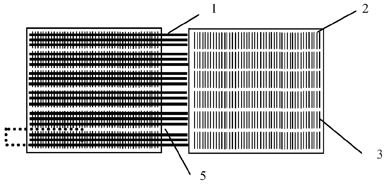
[0043] Such as Figure 2a As shown, an ordinary crystalline silicon photovoltaic cell 9 printed with a pre-broken fine Ag grid line as a metal electrode 3 is connected in series through 18 interconnected metal lines 1 . The interconnection metal wire 1 is connected to the light-receiving surface of the photovoltaic cell 9 on the left side, and is connected to the back side of the photovoltaic cell 9 on the right side at the same time. The interconnection metal wire 1 is composed of Al wire or soft Cu wire coated with Al on the surface.
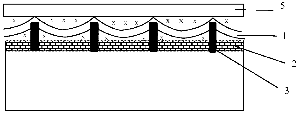
[0044] To illustrate the details of the problem, the Figure 2a The part inside the middle dotted frame is cut off, and viewed from bottom to top along the direction parallel to the paper, the photovoltaic cell structure can be seen as Figure 2b shown.
[0045] Firstly, the electrical connection between the interconnection metal wire 1 and the metal electrode 3 is realized by ultrasonic welding. The ultrasonic frequency is 61kHz, the inte...
Embodiment 2
[0054] Embodiment two: if Figure 2a and 2b As shown, an ordinary crystalline silicon photovoltaic cell 9 printed with a pre-broken fine Ag grid line as a metal electrode 3 is connected in series through 18 interconnected metal lines 1 . The interconnection metal wire 1 is a Cu core wire with an Al alloy surface layer. Other descriptions are the same as in Embodiment 1.
Embodiment 3
[0055] Embodiment 3: In this embodiment, the enhanced multilayer SiNx film replaces the original single-layer SiNx film in Embodiment 1. The Si content of the SiNx film is different in the surface layer and the Si content of the main layer. In the PECVD deposition process of SiNx film, the last 1s process is close to the amorphous silicon deposition process. Others are the same as in Embodiment 1.
PUM
 Abstract
Description
Claims
Application Information
 - R&D
- Intellectual Property
- Life Sciences
- Materials
- Tech Scout
- Unparalleled Data Quality
- Higher Quality Content
- 60% Fewer Hallucinations
Browse by: Latest US Patents, China's latest patents, Technical Efficacy Thesaurus, Application Domain, Technology Topic, Popular Technical Reports.
© 2025 PatSnap. All rights reserved.Legal|Privacy policy|Modern Slavery Act Transparency Statement|Sitemap|About US| Contact US: help@patsnap.com


