Manufacturing method for semiconductor device

A manufacturing method and semiconductor technology, applied in semiconductor/solid-state device manufacturing, semiconductor devices, electric solid-state devices, etc., can solve problems such as damage to reliability, defects, etc.

Inactive Publication Date: 2015-06-17
SYNAPTICS JAPAN GK
View PDF6 Cites 3 Cited by
  • Summary
  • Abstract
  • Description
  • Claims
  • Application Information

AI Technical Summary

Problems solved by technology

It is known that when the ONO film of the MONOS type FET and the polysilicon film as the gate electrode film are formed on the entire surface of the semiconductor substrate, the region where the MOSFET is f

Method used


Image

  • Manufacturing method for semiconductor device
  • Manufacturing method for semiconductor device
  • Manufacturing method for semiconductor device

Examples


Embodiment approach 1

[0130] ﹝Implementation 1﹞

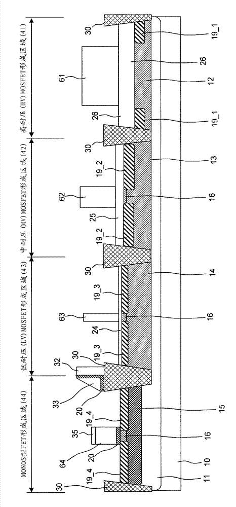
[0131] quote Figure 1 to Figure 20 A method of manufacturing a semiconductor device 1 including: a MONOS-type FET 54 having a charge storage film within a gate insulating film for constituting a nonvolatile memory; Three types of MOSFETs 51 to 53 of high withstand voltage, medium withstand voltage, and low withstand voltage for electrical circuits, analog circuits, and the like.

[0132] figure 1 This is a schematic cross-section of the semiconductor device 1 in the middle of the manufacturing method of the first embodiment (after the N-type well 11 , P-type wells 12 to 14 , P-type channel 16 , and LDD 19_1 for high withstand voltage (HV) MOSFET formation process) picture. A MONOS-type FET formation region 44, a low voltage (LV: Low Voltage) MOSFET formation region 43, a medium voltage (MV: Middle Voltage) MOSFET formation region 42, and a high voltage (HV: High Voltage) MOSFET formation are shown. Area 41. Although only the process of forming...

Embodiment approach 3

[0177] [Embodiment 3]

[0178] It is known that the threshold voltage of the MOSFET may vary when a manufacturing method is employed in which the gate oxide film and the polysilicon film of the MOSFET are formed over the entire surface of the semiconductor substrate, and then the ONO of the MONOS type FET is formed. film and the polysilicon film that forms the gate electrode. The inventors have found through studies that when a silicon oxide film is formed on the polysilicon film formed in step (e) as the gate electrode film of the MOSFET, the threshold voltage of the MOSFET on the P-channel side may vary. As a result of further repeated experiments and studies, the inventors have clarified the fact that such a variation in threshold voltage is particularly significant in a low withstand voltage P-channel MOSFET; and that the formation of the ONO film was omitted in the experiment. In addition, it does not occur in the manufacturing method of forming the ONO film first. Bas...

Embodiment approach 4

[0187] [Embodiment 4]

[0188] Figure 21 is a schematic layout diagram of the MONOS type FET 54 viewed from the upper surface.

[0189] The MONOS-type FET 54 constituting the nonvolatile memory is formed, for example, in a region 45 surrounded by an element isolation region 30 such as an STI, and a gate electrode 64 is formed across the other STI 30 from one STI 30 in the direction of channel width (W). A source region and a drain region are formed along the aforementioned gate electrode 64 . Therefore, in the channel length (L) direction, there are current channels on the inside separated from the sidewall of the STI 30 and current channels along both sides of the sidewall in the vicinity of the sidewall. The inventors have found through studies that the impurity concentration near the side walls of the STI 30 becomes non-uniform or the electric field is disturbed. Therefore, it is possible to show the threshold voltage that dominates the current channel on both sides and...


PUM


Abstract

In a manufacturing method for a semiconductor device provided with a MONOS-type FET for a non-volatile memory and high-voltage and low-voltage MOSFETs, a groove having a predetermined depth is formed in a region in which the high-voltage MOSFET on a semiconductor substrate is formed, and an oxide film serving as a gate insulating film of the high-voltage MOSFET is formed within the formed groove by thermal oxidation. Thereafter, a gate electrode film of the low-voltage MOSFET is formed on the entire surface of the semiconductor substrate. Thereafter, a region for the MONOS-type FET is opened, the semiconductor surface of the semiconductor substrate is exposed, and a first potential barrier film, a charge storage film, and a second potential barrier film are sequentially deposited, to thereby form a charge storage three-layer film. Agate electrode film of the MONOS-type FET is formed on the formed charge storage three-layer film.

Description

technical field [0001] The present invention relates to a method of manufacturing a semiconductor device, and is particularly applicable to a semiconductor device in which a nonvolatile memory and a general MISFET (Metal Insulator Semiconductor Field Effect Transistor: Metal Insulator Semiconductor Field Effect Transistor) are mixed. Background technique [0002] Semiconductor integrated circuits (LSI: Large Scale Integrated Circuit: Large Scale Integrated Circuit) in which nonvolatile memories are mixed with logic circuits, memory circuits, analog circuits, etc. are becoming popular. In logic circuits and the like, silicon oxide (SiO 2 ) film MOSFET (Metal Oxide Semiconductor Field Effect Transistor: Metal Oxide Semiconductor Field Effect Transistor). On the other hand, there is a nonvolatile memory that utilizes a FET having a charge storage film on a gate insulating film among nonvolatile memories. There is a trap level in the charge storage film, and the threshold volt...

Claims


Application Information

Patent Timeline
IPC IPC(8): H01L21/8247H01L21/28
CPCH01L21/26586H01L29/66537H01L21/823462H01L29/792H01L29/4916H01L29/40117H10B43/40
Inventor 石田浩佐藤一彦
Owner SYNAPTICS JAPAN GK
Why Eureka
Try Eureka