Organic light emitting display device and manufacturing method thereof

A light-emitting display and organic technology, applied in semiconductor/solid-state device manufacturing, semiconductor devices, electrical components, etc., can solve the problem that the contact resistance cannot be effectively reduced, and achieve the effects of improving yield, reducing voltage drop, and large contact area

Inactive Publication Date: 2015-06-17
KUNSHAN GO VISIONOX OPTO ELECTRONICS CO LTD
View PDF2 Cites 35 Cited by
  • Summary
  • Abstract
  • Description
  • Claims
  • Application Information

AI Technical Summary

Problems solved by technology

[0008] For this reason, what the present invention aims to solve is the problem that the contact resistance between the second electrode of the organic light emitting diode and the electrode power line canno

Method used


Image

  • Organic light emitting display device and manufacturing method thereof
  • Organic light emitting display device and manufacturing method thereof
  • Organic light emitting display device and manufacturing method thereof

Examples


Example Embodiment

[0042] Example

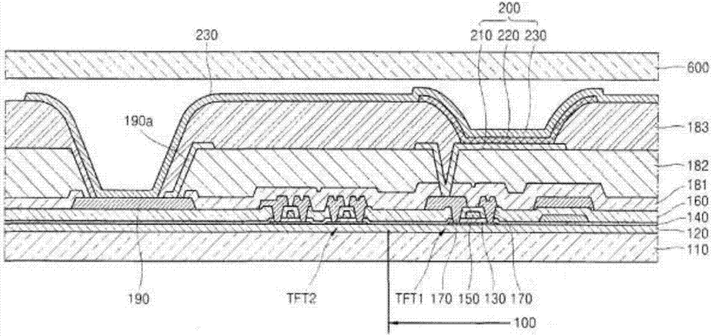
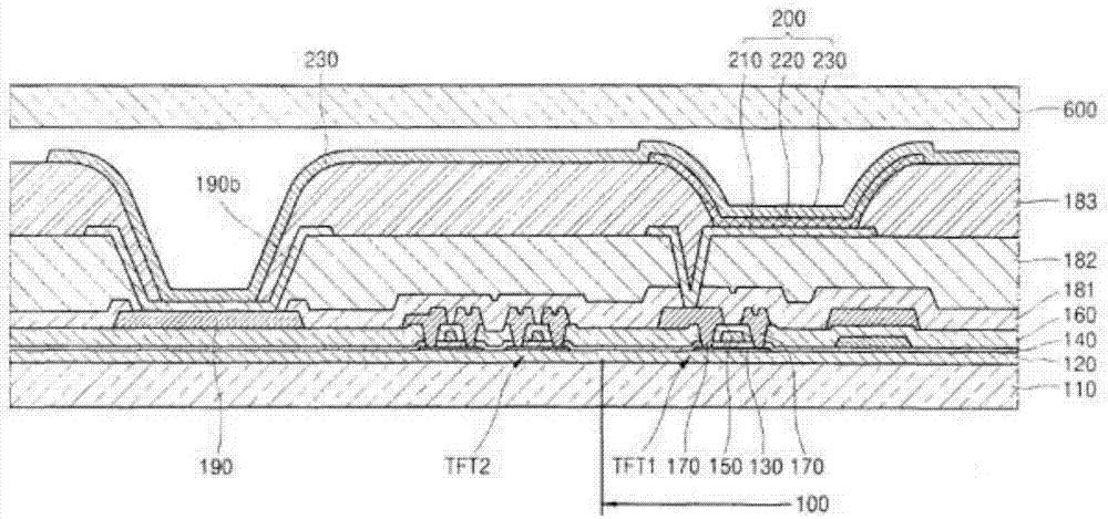
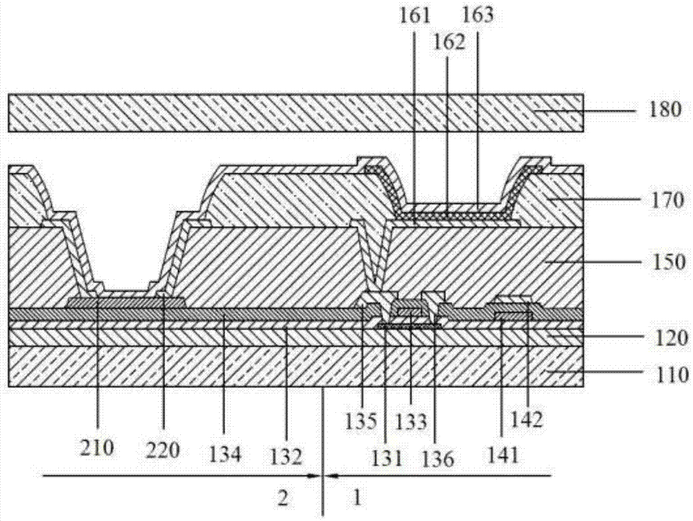
[0043] This embodiment provides an organic light emitting display device, such as image 3 As shown, it includes a substrate 110, thin film transistors, capacitors and organic light emitting diodes arranged in the display area 1 of the substrate, and electrode power lines 210 arranged in the non-display area 2 of the substrate 110.

[0044] The substrate 110 is selected from but not limited to a glass substrate or a polymer substrate, and a glass substrate is preferred in this embodiment.

[0045] A buffer layer 120 is directly formed on the substrate 110. The buffer layer is selected from but not limited to a one-layer or multi-layer stack structure formed by silicon oxide and / or silicon nitride, and has a thickness of 40-400 nm. This embodiment Preferably, the silicon oxide layer has a thickness of 230 nm.

[0046] The organic light emitting diode includes a first electrode 161, an organic light emitting layer 162, and a second electrode 163 stacked in sequence. Th...


PUM

PropertyMeasurementUnit
Thicknessaaaaaaaaaa
Thicknessaaaaaaaaaa
Thicknessaaaaaaaaaa

Abstract

The invention discloses an organic light emitting display device. An auxiliary conductive layer is directly formed on an electrode power line and is exposed out of partial region of the electrode power line; and a second electrode extends to the non-display region and continuously covers the surface, away from the electrode power line, of the auxiliary conductive layer and the exposed surface of the electrode power line. The areas where the second electrode is contacted with the electrode power line and the auxiliary conductive layer are large, the electrode power line thus can easily build a short conductive path via the auxiliary conductive layer, contact resistance between the second electrode and the electrode power line can be effectively reduced, and voltage drop between the electrode power line and the second electrode is reduced. According to the organic light emitting display device manufacturing method disclosed by the invention, the technology is simple, and the manufacturing cost is low.

Description

technical field [0001] The invention relates to the field of organic electroluminescence, in particular to an organic light-emitting display device capable of reducing the resistance of an electrode power line (VSS) and a preparation method thereof. Background technique [0002] Flat panel display has the characteristics of complete planarization, lightness, thinness, and power saving. It is an inevitable trend and research focus of image display development. Among various types of flat panel display devices, since the active matrix organic light emitting display device (English full name is Active Matrix Organic Light Emitting Display, referred to as AMOLED) uses self-luminous organic light emitting diode (English full name is Organic Light Emitting Diode, referred to as OLED). ) to display images, has the characteristics of short response time, driving with low power consumption, and relatively better brightness and color purity, so organic light-emitting display devices h...

Claims


Application Information

Patent Timeline
IPC IPC(8): H01L27/32H01L51/56
Inventor 赵雁飞李建文魏博陈浩陈策
Owner KUNSHAN GO VISIONOX OPTO ELECTRONICS CO LTD
Why Eureka
Try Eureka