Film deposition equipment

A technology of thin film deposition and equipment, applied in the field of thin film deposition equipment, can solve the problems of unstable performance of ITO thin films, unstable luminous efficiency and overall electrical performance of LED devices, etc., and achieve the effect of improving production efficiency and stabilizing performance.

Inactive Publication Date: 2015-07-01
BEIJING NAURA MICROELECTRONICS EQUIP CO LTD
View PDF4 Cites 3 Cited by
  • Summary
  • Abstract
  • Description
  • Claims
  • Application Information

AI Technical Summary

Problems solved by technology

Thereby, when the above-mentioned PVD equipment controls the deposition rate of the ITO film on the substrate 5, the Rs resistance and the transmittance of the ITO film will have a large change, so that the performance of the ITO film is very unstable, that is: the ITO film with the same thickness The thin film has different thin film properties, which makes the luminous efficiency and overall electrical performance of the LED device using the thin film unstable

Method used


Image

  • Film deposition equipment
  • Film deposition equipment
  • Film deposition equipment

Examples


Embodiment Construction

[0024] In order to enable those skilled in the art to better understand the technical solution of the present invention, the thin film deposition equipment provided by the present invention will be described in detail below with reference to the accompanying drawings.

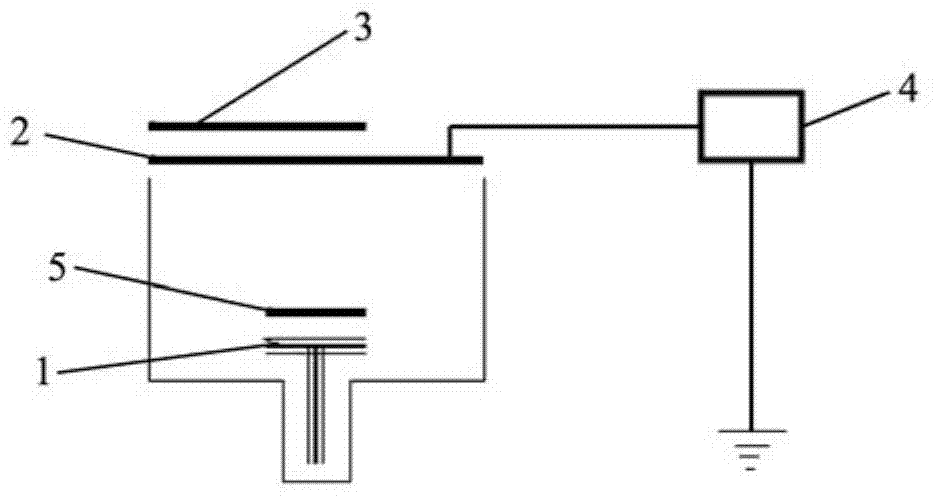
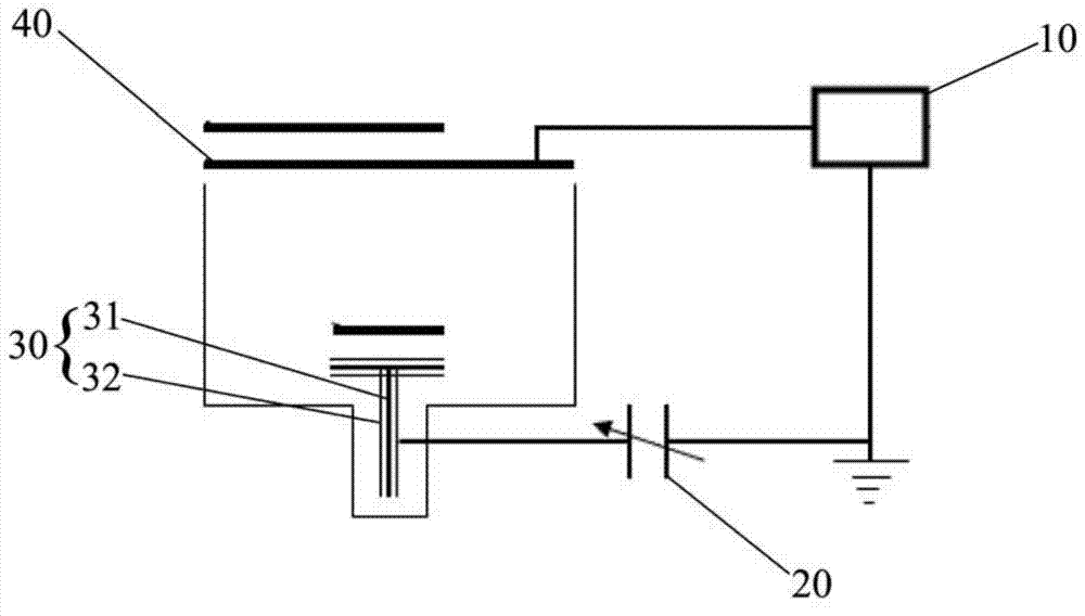
[0025] figure 2 It is a schematic structural diagram of the thin film deposition equipment provided by the first embodiment of the present invention. Please see figure 2 , the film deposition equipment includes a reaction chamber, an excitation power source 10 and a variable capacitor 20 . Wherein, the reaction chamber includes a supporting device 30 and a target 40 ; in this embodiment, the target 40 is an ITO target, which is arranged on the top of the reaction chamber and is electrically connected to the excitation power source 10 . The carrying device 30 is arranged in the reaction chamber and is located at a position corresponding to the target 40 for carrying the substrate; specifically, the carrying ...


PUM


Abstract

The invention relates to film deposition equipment, which comprises a reaction cavity, an excitation power supply and a variable capacitor; the reaction cavity comprises a bearing apparatus and a target material, the target material is arranged at top of the reaction cavity and is electrically connected to the excitation power supply; the bearing apparatus is arranged in the reaction chamber and is positioned at a part corresponding to the target material for bearing a substrate; one end of the variable capacitor is connected to the bearing apparatus, and the other end is connected to ground. The film deposition equipment can control the deposition rate of the film deposited on the substrate by changing the capacitance value of the variable capacitor; under the controlled different film deposition rates, the performance of the film deposited on the substrate is essentially constant.

Description

technical field [0001] The invention relates to the field of semiconductor equipment manufacturing, in particular to a thin film deposition equipment. Background technique [0002] Indium tin oxide (Indium tin oxide, hereinafter referred to as ITO) film has extremely high transparency, its transmittance in visible light can reach more than 90%, and it also has good electrical conductivity. In addition, it also has an extended surface Therefore, ITO thin films are widely used in light emitting diode (Light emitting diode, hereinafter referred to as LED) devices to improve the luminous efficiency and overall electrical performance of LED. [0003] In actual use, physical vapor deposition (Physical Vapor Deposition, hereinafter referred to as PVD) equipment is generally used to deposit an ITO film on the surface of the substrate. figure 1 It is a structural schematic diagram of a reaction chamber of an existing PVD device for depositing an ITO thin film on a substrate surface....

Claims


Application Information

Patent Timeline
Patent Type & Authority Applications(China)
IPC IPC(8): C23C14/35C23C14/08
Inventor 田立飞耿波文莉辉张同文王厚工丁培军
Owner BEIJING NAURA MICROELECTRONICS EQUIP CO LTD
Why Eureka
Try Eureka