

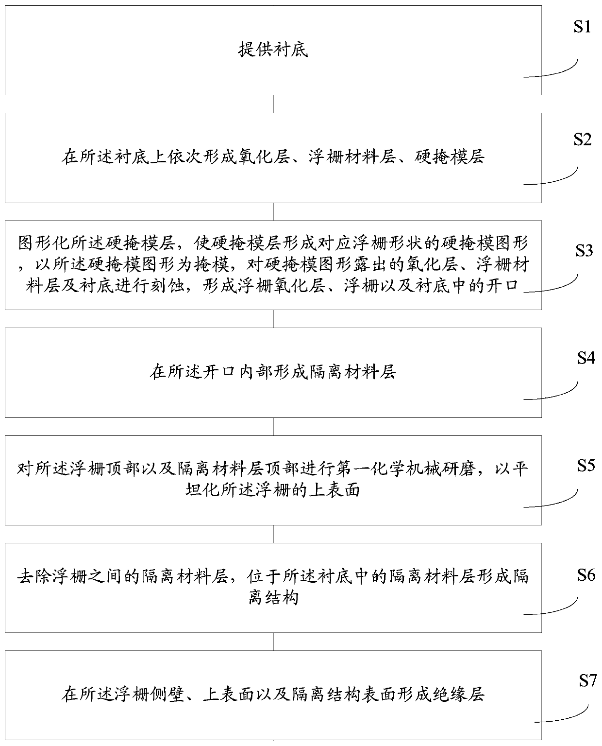
Method of forming memory
A memory and graphics technology, applied in semiconductor devices, electric solid devices, electrical components, etc., can solve the problem of poor storage capacity of floating gates, achieve high flatness, uniform thickness, and improve the ability to hold charges.
- Summary
- Abstract
- Description
- Claims
- Application Information
AI Technical Summary
Problems solved by technology
Method used
Image

Examples
Embodiment Construction
[0032] With the shrinking of the semiconductor feature size, the thickness of the insulating layer in the memory, especially in ETOX, is constantly decreasing. It often occurs that the local electric field strength near the insulating layer is greater than the surrounding electric field strength, which makes the ability of the floating gate to hold charges worse.
[0033] The phenomenon that the local electric field intensity near the insulating layer of the existing technology is greater than the intensity of the surrounding electric field is analyzed. The uniformity is poor, causing the local electric field strength near the insulating layer to be greater than that of the surrounding electric field.
[0034] In order to solve the technical problem, the present invention provides a method for forming a memory, using a self-aligned isolation structure process, after forming the floating gate and the isolation material layer between the floating gates, the top of the floating ga...
PUM
 Abstract
Description
Claims
Application Information