Up-conversion-nanocrystal-based stimulated depletion super-resolution optical microscopic method and up-conversion-nanocrystal-based stimulated depletion super-resolution optical microscopic system

A stimulated loss, optical microscopy technology, applied in the field of optical microscopy and optical nanomaterials, can solve the problems of small wavelength interval of excitation light detection fluorescence, high cost investment, eliminate autofluorescence interference, improve imaging depth, Avoid flickering effects

Inactive Publication Date: 2015-07-08
SOUTH CHINA NORMAL UNIVERSITY
View PDF9 Cites 24 Cited by
  • Summary
  • Abstract
  • Description
  • Claims
  • Application Information

AI Technical Summary

Problems solved by technology

The excitation light in the above expression is generally femtosecond pulse laser or continuous (CW) laser, and the loss light is generally high-power laser (for example, femtosecond pulse laser or high-power CW laser), because the use of pulse laser requires a series of complex and expensive components, and the wavelength intervals of excitation light, loss light, and detection fluorescence are very small, so this type of device has the disadvantage of high cost investment

Method used


Image

  • Up-conversion-nanocrystal-based stimulated depletion super-resolution optical microscopic method and up-conversion-nanocrystal-based stimulated depletion super-resolution optical microscopic system
  • Up-conversion-nanocrystal-based stimulated depletion super-resolution optical microscopic method and up-conversion-nanocrystal-based stimulated depletion super-resolution optical microscopic system
  • Up-conversion-nanocrystal-based stimulated depletion super-resolution optical microscopic method and up-conversion-nanocrystal-based stimulated depletion super-resolution optical microscopic system

Examples


Embodiment 1

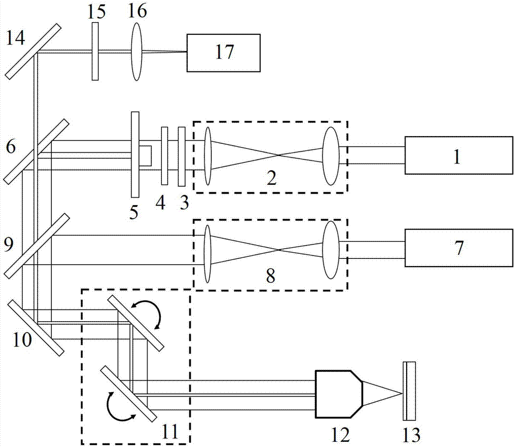
[0039] like figure 1 As shown, the stimulated depletion super-resolution optical microscopy system based on up-conversion nanocrystals includes a depletion light generation module, an excitation light generation module, a collimating coaxial coupling module composed of two dichroic mirrors, and a multiphoton microscope A scanning module and a photoelectric detection module.

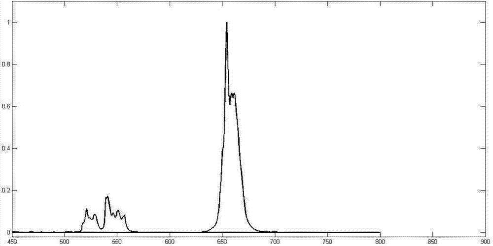
[0040] This example uses NaYF 4 :Yb 3+ / Er 3+ As fluorescent markers for upconverting materials, see figure 2 , its photoluminescent fluorescence spectrum has two emission peaks at 532nm and 655nm, so this embodiment adopts the first continuous laser 1 with a center wavelength of 532nm, and the laser emitted by it is phase-modulated by a spatial phase modulation plate to form a hollow beam as For the stimulated depletion light, the second continuous laser 7 with a center wavelength of 975nm is used as the excitation light of the fluorescent marker to detect the super-resolution two-photon fluorescenc...

Embodiment 2

[0046] Present embodiment except following feature other structures are with embodiment 1:

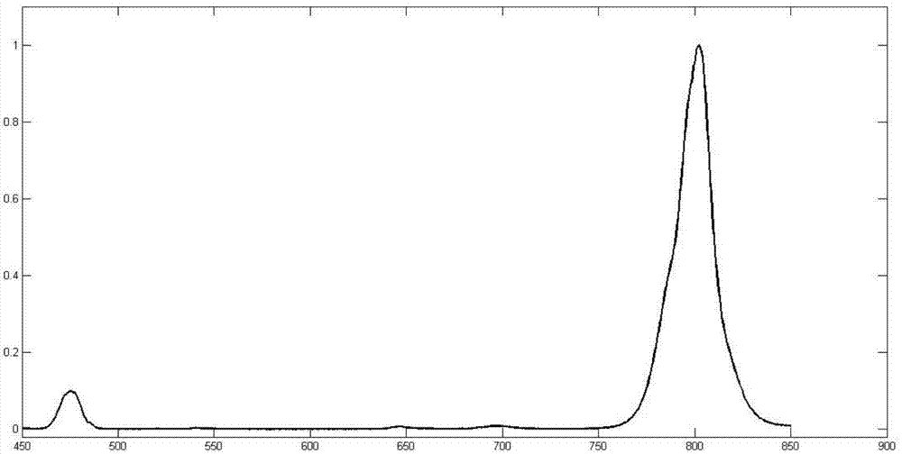
[0047] Depend on image 3 As shown, this embodiment uses NaYF 4 :Yb 3+ / Tm 3+ As an up-conversion material fluorescent marker, its photoluminescence fluorescence spectrum has two emission peaks at 480nm and 800nm, so the first continuous laser with a center wavelength of 800nm ​​is used to form a hollow beam after phase modulation by a spatial phase modulation plate as the stimulated For loss of light, the second continuous laser with a center wavelength of 975nm is used as the excitation light of the fluorescent marker, and the photodetection module detects the 480nm super-resolution two-photon fluorescence signal generated by the above-mentioned two laser beams collimated, coaxially coupled, focused and scanned. Obtain fluorescence imaging.

[0048] In this embodiment, the critical wavelengths of the high-transmission and low-transmission anti-dichroic mirror and the low-transmis...

Embodiment 3

[0050] Present embodiment except following feature other structures are with embodiment 1:

[0051] Depend on Figure 5 As shown, this embodiment uses NaYF 4 :Er 3+ As a fluorescent marker for upconversion materials, Er 3+ As a sensitizing ion and an activating ion at the same time, its photoluminescence fluorescence spectrum energy level structure has two emission peaks at 655nm and 545nm, and the excitation light energy level difference is as follows: Figure 5 As shown, the first continuous laser with a central wavelength of 655nm is used as a hollow beam after phase modulation by a spatial phase modulation plate as the stimulated loss light, and the second continuous laser with a central wavelength of 1490nm is used as the excitation light for fluorescent markers. The detection module detects the 545nm super-resolution three-photon fluorescence signal generated by the above-mentioned two laser beams collimated, coaxially coupled, focused and scanned to obtain fluorescen...


PUM


Abstract

The invention discloses an up-conversion-nanocrystal-based stimulated depletion super-resolution optical microscopic method and an up-conversion-nanocrystal-based stimulated depletion super-resolution optical microscopic system. An up-conversion nanocrystal and the stimulated emission depletion super-resolution fluorescence micro-imaging technique are combined, a super-resolution multiphoton fluorescence signal generated by stimulated emission depletion of an up-conversion luminescent nanometer material labeled sample is detected, a continuous low-power steady-state stimulated depletion process of multiphotons excited by a laser is realized and the simple and effective three-dimensional super-resolution imaging effect having low cost, low complexity and high resolution can be achieved. The stimulated emission depletion super-resolution optical micro-imaging system composed of a depletion light generating module, an exciting light generating module, a plurality of dichroscopes, a multiphoton micro-scanning module and a photoelectric detection module is built based on the method, and a simple and effective real-time dynamic three-dimensional image having low cost, low complexity and high resolution can be acquired.

Description

technical field [0001] The invention relates to the fields of optical microscopy technology and optical nanomaterials, in particular to a stimulated loss super-resolution optical microscopy method and system based on up-conversion nanocrystals. Background technique [0002] According to the Rayleigh / Abbe criterion, the distance between two equal luminances that the optical system can distinguish corresponds to the radius of the Airy disk, and the size of the Airy disk can be expressed as: [0003] Δr = 0.61 λ NA [0004] Where λ is the wavelength of the incident light, and NA is the numerical aperture of the lens. Then, the limit resolution of the conventional optical system is in the half-wavelength range. [0005] Stimulated Emission Depletion Microscopy (STED) is a super-resolution imaging method that utilizes the nonlinear relationship between fluorescence saturation and stimu...

Claims


Application Information

Patent Timeline
Patent Type & Authority Applications(China)
IPC IPC(8): G01N21/64
Inventor 詹求强何赛灵杨东尼林众宇潘江帆
Owner SOUTH CHINA NORMAL UNIVERSITY
Why Eureka
Try Eureka