Logic device based on spin wave interference and multiferroic material
A logic device and spin wave technology, applied in the structural design and functional application of logic devices, can solve problems such as high energy consumption and low reliability, reduce difficulty, ensure stable existence, and eliminate instability and energy loss. Effect
- Summary
- Abstract
- Description
- Claims
- Application Information
AI Technical Summary
Problems solved by technology
Method used
Image
Examples
Embodiment Construction
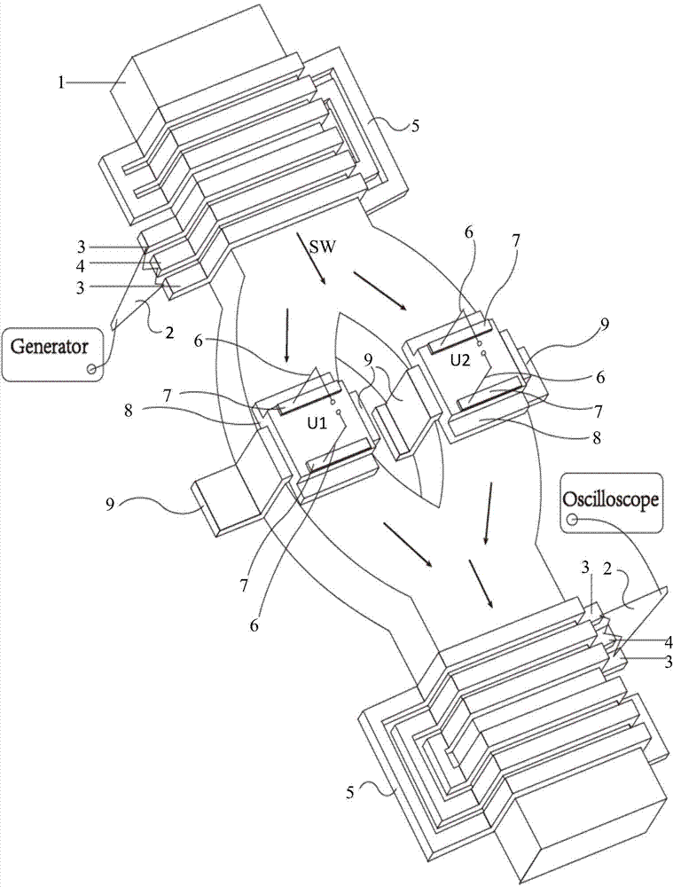
[0027] The invention proposes a logic device based on spin wave interference and multiferroic materials, which can be used for information transmission and logic operation. The logic device is composed of a spin wave excitation area, a spin wave frequency division area, an electric field regulation area, a spin wave interference area and a spin wave detection area. The attached drawings are all schematic diagrams, and the size and thickness of the functional areas involved are not actual sizes, and the current and wavelength in the working mode are also not actual values. There are also many choices of materials, depending on actual needs.
[0028] The spin wave transmission medium can be in any shape, depending on the specific application, and the size can be measured from a few nanometers to hundreds of microns. Most of the materials are ferromagnetic materials, which can be selected from but not limited to the following materials: Permalloy, cobalt iron boron (CoFeB), yttri...
PUM
 Abstract
Description
Claims
Application Information


