C/(SiC/BN)n compound interface phase coating, coating fiber and preparation method of coating fiber
A coating fiber and interfacial phase technology, which is applied in the field of composite interfacial phase coating and its preparation, can solve the problems of material performance degradation, limited service temperature, performance degradation, etc., and achieve the effect of improving damage tolerance and increasing toughness
- Summary
- Abstract
- Description
- Claims
- Application Information
AI Technical Summary
Problems solved by technology
Method used
Image
Examples
Embodiment 1
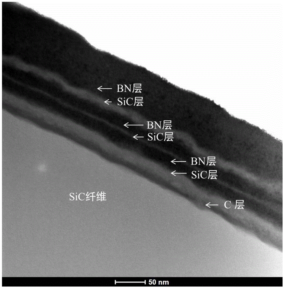
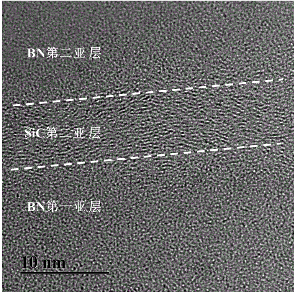
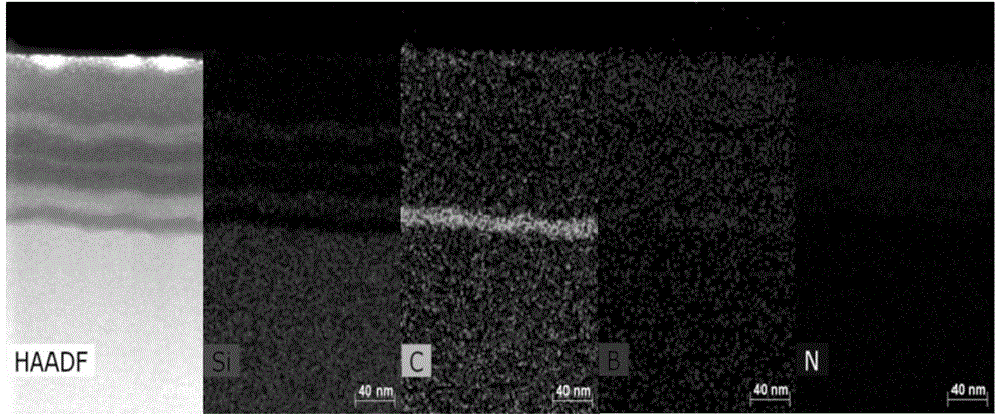
[0031] Such as figure 1 , figure 2 , image 3 As shown, the C / (SiC / BN) between a silicon carbide fiber and a matrix that can be used as a ceramic matrix composite material of the present invention n Composite interfacial phase coating, the composite interfacial phase coating has a periodic stacked structure, the periodic stacked structure specifically refers to the alternating periodic stacking of SiC layers and BN layers, the stacked layers of periodic stacking in this embodiment The number of cycles is 3 times. Specifically, the thickness of the C layer from the inside to the outside is 20.0nm, the thickness of the first sublayer of SiC is 25.0nm, the thickness of the first sublayer of BN is 25.0nm, the thickness of the second sublayer of SiC is 8.0nm, and the thickness of the first sublayer of BN is 8.0nm. The thickness of the second sublayer is 20.0nm, the thickness of the third sublayer of SiC is 20.0nm, and the thickness of the third sublayer of BN is 50.0nm.
[003...
Embodiment 2
[0044] A kind of C / (SiC / BN) between silicon carbide fiber and matrix that can be used as ceramic matrix composite material of the present invention n Composite interfacial phase coating, the composite interfacial phase coating has a periodic stacked structure, the periodic stacked structure specifically refers to the alternating periodic stacking of SiC layers and BN layers, the stacked layers of periodic stacking in this embodiment The number of cycles is 5 times. Specifically, the thickness of the C layer from the inside to the outside is 15.0nm, the thickness of the first sublayer of SiC is 8.0nm, the thickness of the first sublayer of BN is 20.0nm, the thickness of the second sublayer of SiC is 18.0nm, and the thickness of the first sublayer of BN is 18.0nm. The thickness of the second sublayer is 25.0nm, the thickness of the third sublayer of SiC is 25.0nm, the thickness of the third sublayer of BN is 50.0nm, the thickness of the fourth sublayer of SiC is 25.0nm, and the ...
PUM
| Property | Measurement | Unit |
|---|---|---|
| Thickness | aaaaa | aaaaa |
| Thickness | aaaaa | aaaaa |
| Thickness | aaaaa | aaaaa |
Abstract
Description
Claims
Application Information


