Silicon substrate electro-optical OR-AND integrated logic device

A technology for integrating electro-optic and logic devices, which is applied in the direction of logic circuits, electrical components, and logic circuits using optoelectronic devices, to achieve good flexibility and universality, easy integration, and small device size

Inactive Publication Date: 2015-07-22
INST OF SEMICONDUCTORS - CHINESE ACAD OF SCI
View PDF0 Cites 2 Cited by
  • Summary
  • Abstract
  • Description
  • Claims
  • Application Information

AI Technical Summary

Problems solved by technology

The electro-optic logic device takes full advantage of the advantages of silicon-based waveguide, such as compact structure, low power consumption, and compatibility with CMOS technology, and solves the integration and miniaturization problems of reconfigurable electro-optic guided logic devices.

Method used


Image

  • Silicon substrate electro-optical OR-AND integrated logic device
  • Silicon substrate electro-optical OR-AND integrated logic device
  • Silicon substrate electro-optical OR-AND integrated logic device

Examples


Embodiment Construction

[0030] It should be noted that, in the drawings or descriptions of the specification, similar or identical parts all use the same figure numbers. Implementations not shown or described in the accompanying drawings are forms known to those of ordinary skill in the art. Additionally, while illustrations of parameters including particular values ​​may be provided herein, it should be understood that the parameters need not be exactly equal to the corresponding values, but rather may approximate the corresponding values ​​within acceptable error margins or design constraints. In addition, the directional terms mentioned in the following embodiments, such as "upper", "lower", "front", "rear", "left", "right", etc., are only referring to the directions of the drawings. Accordingly, the directional terms are used to illustrate and not to limit the invention.

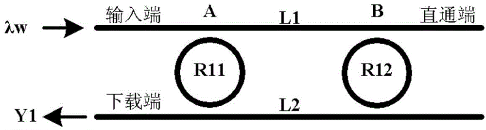
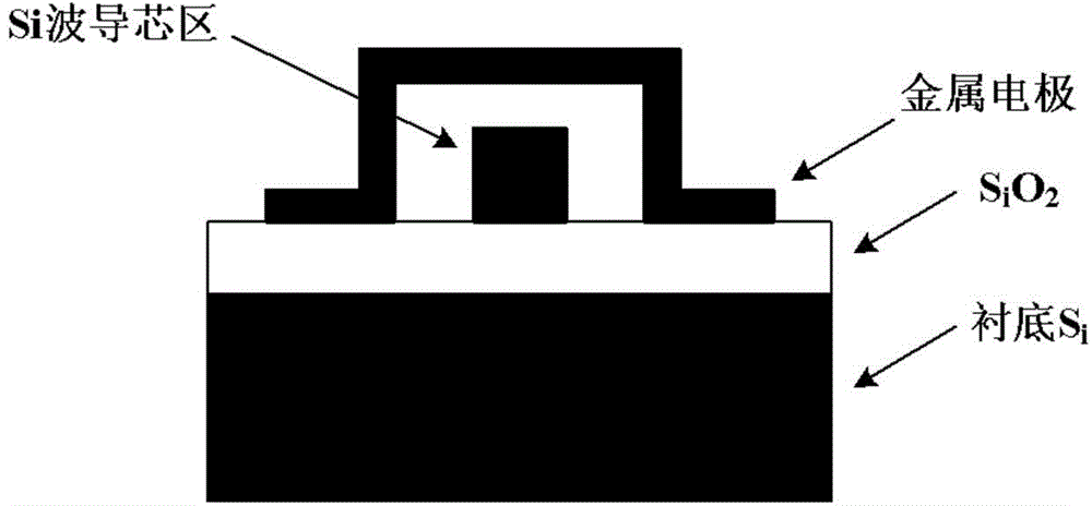
[0031] What the present invention adopts aspect material processing is silicon on insulator (Silicon on Insulator, SOI) tech...


PUM


Abstract

The invention discloses a silicon substrate electro-optical OR-AND integrated logic device used for realizing any logic functions of two input variables, including AND NAND OR NOR Not Exclusive Or and XOR. The silicon substrate electro-optical OR-AND integrated logic device is formed by connecting two maximum term structures through a transition waveguide in a cascading mode. Each maximum term structure is composed of two micro-ring resonators and two straight waveguides to realize the maximum terms and of the two input variables. The silicon substrate electro-optical OR-AND integrated logic device is made of silicon material on an insulator, is machined through the existing CMOS technology, and is small in size, low in power consumption, low in cost and capable of being conveniently integrated with electric elements.

Description

technical field [0001] The invention belongs to the field of optical information processing and optical calculation, and in particular relates to an integrated electro-optic OR and logic device based on a silicon-based nanowire waveguide that can realize any logic function of two input variables. Background technique [0002] Optical information processing technology has the advantages of high processing parallelism, low crosstalk, large bandwidth, and low power consumption, and will play an important role in large-scale data processing and data interconnection in the future. As an important unit of future optical computers, optical logic devices have made great progress in recent years. In 2007, American scientist James Hardy and Israeli scientist Joseph Shamir proposed the concept of electro-optical guided logic (“Optics inspired logic architecture”, Optics Express, Vol.15, Issue 1, 2007, pp.150-165). The basic idea is to use the electrical signal operand to control the s...

Claims


Application Information

Patent Timeline
IPC IPC(8): G02F3/00
CPCG02F3/00
Inventor 周平杨林张磊丁建峰陈乔杉
Owner INST OF SEMICONDUCTORS - CHINESE ACAD OF SCI
Why Eureka
Try Eureka