Capacitive touch screen and preparation method

A technology of capacitive touch screen and sensing electrode, which is applied in the direction of electrical digital data processing, instrumentation, data processing input/output process, etc., can solve the problems of long cycle, many equipments, and increasing process difficulty, and achieve overall thickness reduction and simplification Etching process, the effect of reducing production costs

Inactive Publication Date: 2015-07-29
FUJIAN HUIRUI TOUCH TECH
View PDF3 Cites 10 Cited by
  • Summary
  • Abstract
  • Description
  • Claims
  • Application Information

AI Technical Summary

Problems solved by technology

Moreover, the G+G / G+F structure has the following disadvantages: the former is relatively thick and heavy, and cannot achieve light and thin effects, and requires the use of bridging or jumper processes, which virtually increases the difficulty of the process and requires high precision; The latter structure is rarely used due to the increased risk of product reliability due to the use of the above process
Using yellow photolithography, acid etching, or etching paste etching is cumbersome, long-term, and pollutes the environment. Especially, the conductive pattern using ITO plus metal wiring needs to be etched multiple times due to different conductive substances. Or printing silver paste after etching, resulting in high production cost of touch screen, low production yield, many and complicated equipment, and high production environment requirements. With the increasingly fierce market competition, the cost pressure is becoming increasingly prominent. The requirement to simplify the process and reduce costs has become Urgent requirements in the field of touch screen

Method used


Image

  • Capacitive touch screen and preparation method
  • Capacitive touch screen and preparation method
  • Capacitive touch screen and preparation method

Examples


Embodiment 1

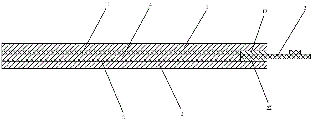
[0030] The driving electrode layer 21 in the present embodiment is a graphene sensing electrode layer, the film layer 2 is a PET film layer, and the thickness of the panel layer 1 is 0.5mm; the thickness of the film layer 2 is 0.1mm; the thickness of the transparent insulating adhesive layer 4 is 0.05mm.

Embodiment 2

[0032] The driving electrode layer 21 in the present embodiment is the induction electrode layer that graphene and ITO mix, and film layer 2 is PMMA layer, and the thickness of glass panel layer 1 is 0.7mm; The thickness of film layer 2 is 0.3mm; Transparent insulating adhesive layer 4 has a thickness of 0.2mm.

[0033] In practical applications, the driving electrode layer 21 can also be a metal mesh wire sensing electrode layer or an ITO sensing electrode layer.

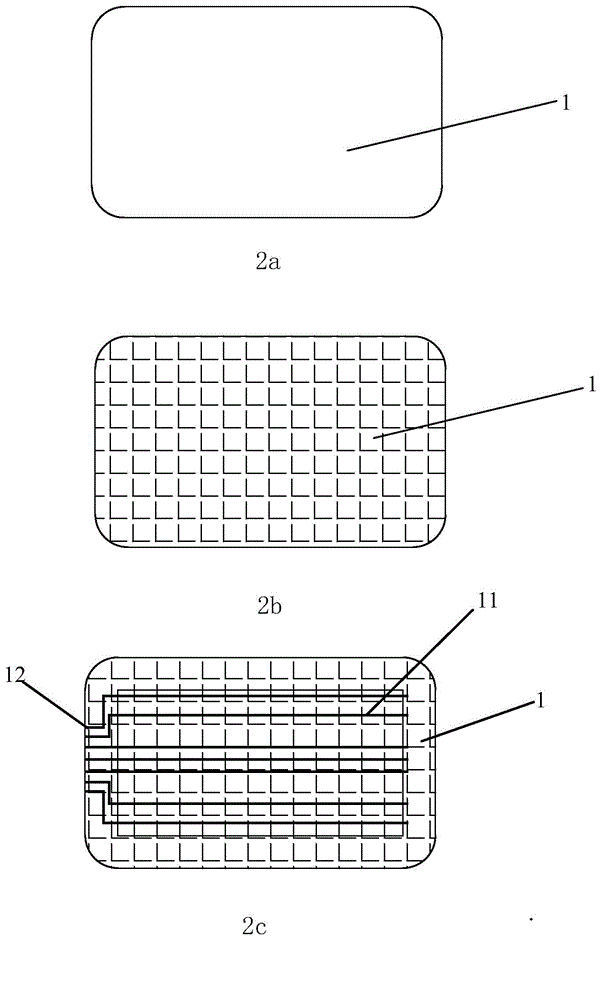
[0034] Such as figure 2 Shown, the preparation method of a kind of capacitive touch screen of the present invention, it comprises the following steps:

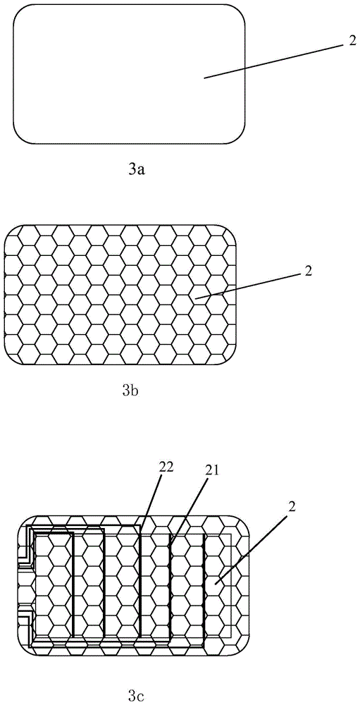
[0035] Sputtering the first conductive film layer on the surface of glass panel layer 1 (such as figure 2 2b in ), and at the same time generate a second conductive film layer on the surface of the film layer 2 (such as image 3 3b) in which the process vacuum during sputtering is between 0.05 and 1Pa, and the sputtering power density is between 1 and 5W / cm 2...

Embodiment 3

[0049] In this embodiment, when sputtering the first conductive film layer on the surface of the glass panel layer 1 and generating the second conductive film layer on the surface of the film layer 2, the process vacuum is 0.6Pa, and the sputtering power density is 4W / cm2; After the first conductive film layer is sputtered on the surface of the glass panel layer 1, and after the second conductive film layer is sputtered on the surface of the thin film layer 2 and before the laser etching is carried out to the first conductive film and the second conductive film, also The method comprises the step of printing a silver paste layer on the first conductive film and the second conductive film, so that the channel resistance of the touch screen meets the requirement.

[0050] When the first conductive film layer is laser etched to form the sensing electrode layer 11, and the second conductive film layer is laser etched to form the driving electrode layer 21, the laser power is 13W; ...


PUM

PropertyMeasurementUnit
diameteraaaaaaaaaa
thicknessaaaaaaaaaa
thicknessaaaaaaaaaa

Abstract

The invention discloses a capacitive touch screen and a preparation method. The capacitive touch screen comprises a glass panel layer, a film layer and a flexible circuit board, wherein the glass panel layer and the film layer are sequentially laminated from top to bottom, the lower surface of the glass panel layer is provided with an induction electrode layer and an induction electrode outgoing line layer, and the induction electrode outgoing line layer is an ITO (Indium Tin Oxide) induction electrode layer; the upper surface of the film layer is provided with a drive electrode layer and a drive electrode outgoing line layer, the surface of glass panel layer provided with the induction electrode layer and the surface of the film layer provided with the drive electrode layer are mutually glued through a transparent insulating glue layer, and the induction electrode outgoing line layer and the drive electrode outgoing line layer are connected in such a way that the front sides and reverse sides are bonded through the flexible circuit board. According to the capacitive touch screen provided by the invention, the induction electrode layer and the drive electrode layer can be etched by a laser etching technology, and the relevant parameters can be regulated to etch a conducting film and relevant leads better, therefore the etching process can be simplified, the process yield can be greatly improved, and the production cost can be reduced.

Description

technical field [0001] The invention relates to the field of touch screens, in particular to a capacitive touch screen and a preparation method. Background technique [0002] The touch screen is an input device that can facilitate the interaction between people and computers and other portable mobile devices. In recent years, capacitive touch screens based on indium tin oxide (ITO) transparent conductive films, especially projected capacitive screens, which can perform multi-finger recognition and realize multi-touch, have been widely used in mobile Internet devices, such as smart phones and portable tablet computers. . [0003] At present, the mainstream projected capacitive screens on the market mainly include G+G / G+F and G+F+F structures according to their structure. The projected capacitive screens with G+G structure include cover glass, adhesive layer and conductive glass. The total thickness is about 1.4mm; the G+F structure includes cover glass, adhesive layer and c...

Claims


Application Information

Patent Timeline
Patent Type & Authority Applications(China)
IPC IPC(8): G06F3/044
Inventor 杨与胜
Owner FUJIAN HUIRUI TOUCH TECH
Why Eureka
Try Eureka