Preparation method of N-type low-drift-angle silicon carbide epitaxial wafer
A technology of low-off-angle silicon carbide and epitaxial wafers, applied in semiconductor/solid-state device manufacturing, electrical components, circuits, etc., can solve problems such as difficult control of surface roughness, achieve extended cleaning cycle, reduce basal plane dislocation density, The effect of reducing the cost of growth
- Summary
- Abstract
- Description
- Claims
- Application Information
AI Technical Summary
Problems solved by technology
Method used
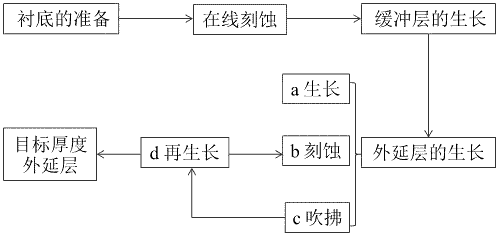
Image

Examples
Embodiment 1
[0040] A method for preparing an N-type low off-angle silicon carbide epitaxial wafer with a thickness of 15 μm, comprising the following steps:
[0041] 1) On-line etching substrate: Prepare a 4H-SiC substrate with an off angle of 4°, vacuumize it, and feed in hydrogen gas at a flow rate of 40L / min and HCl at a flow rate of 5L / min. The pressure in the reaction chamber is 40mbar and the temperature is 1680°C , for 5 minutes;
[0042] 2) Growth of the buffer layer: Stop feeding HCl, lower the temperature to 1650°C, and feed SiH with a flow rate of 6mL / min 4 and 3mL / min of C 3 h 8 , with the flow rate of 1500mL / min N 2 As a dopant, the growth pressure is 40mbar, and a buffer layer with a thickness of 0.4μm is grown;
[0043] 3) Growth of epitaxial layer
[0044] a Growth: 40L / min flow rate of hydrogen, 10mL / min SiH 4 and 5mL / min of C 3 h 8 Pass into the reaction chamber, keep the temperature at 1650°C, the pressure at 40mbar, and the N at a flow rate of 800mL / min 2 As a...
Embodiment 2
[0049] A method for preparing N-type low off-angle silicon carbide epitaxy with a thickness of 30 μm, comprising the following steps:
[0050] 1) On-line etching of the substrate: prepare a 4H-SiC substrate with an off-angle of 2°, vacuumize it, feed in hydrogen gas at a flow rate of 40L / min and HCl at a flow rate of 5L / min, the pressure in the reaction chamber is 40mbar, and the temperature is 1680°C , for 5 minutes;
[0051] 2) Growth of the buffer layer: Stop feeding HCl, lower the temperature to 1650°C, and feed SiH with a flow rate of 6mL / min 4 and 3mL / min of C 3 h 8 , with the flow rate of 1500mL / min N 2 As a dopant, the growth pressure is 40mbar, and a buffer layer with a thickness of 1 μm is grown;
[0052] 3) Growth of epitaxial layer
[0053] a Growth: 40L / min flow rate of hydrogen, 10mL / min SiH 4 and 5mL / min of C 3 h 8 Pass into the reaction chamber, keep the temperature at 1650°C, the pressure at 40mbar, and the N at a flow rate of 800mL / min 2 As a dopant, g...
Embodiment 3
[0061] A method for preparing N-type low off-angle silicon carbide epitaxy with a thickness of 80 μm, comprising the following steps:
[0062] 1) On-line etching of the substrate: Prepare a 4H-SiC substrate with an off-angle of 4°, vacuumize it, and feed in hydrogen gas at a flow rate of 40L / min and HCl at a rate of 5L / min. The pressure in the reaction chamber is 40mbar and the temperature is 1680°C , for 5 minutes;
[0063] 2) Growth of the buffer layer: Stop feeding HCl, lower the temperature to 1650°C, and feed SiH with a flow rate of 6mL / min 4 and 3mL / min of C 3 h 8 , with the flow rate of 1500mL / min N 2 As a dopant, the growth pressure is 40mbar, and a 1.5μm thick buffer layer is grown;
[0064] 3) Growth of epitaxial layer
[0065] a Growth: 40L / min flow rate of hydrogen, 10mL / min SiH 4 and 5mL / min of C 3 h 8 Pass into the reaction chamber, keep the temperature at 1650°C, the pressure at 40mbar, and the N at a flow rate of 800mL / min 2 As a dopant, grow a 10μm th...
PUM
| Property | Measurement | Unit |
|---|---|---|
| thickness | aaaaa | aaaaa |
| thickness | aaaaa | aaaaa |
| thickness | aaaaa | aaaaa |
Abstract
Description
Claims
Application Information
 - R&D
- Intellectual Property
- Life Sciences
- Materials
- Tech Scout
- Unparalleled Data Quality
- Higher Quality Content
- 60% Fewer Hallucinations
Browse by: Latest US Patents, China's latest patents, Technical Efficacy Thesaurus, Application Domain, Technology Topic, Popular Technical Reports.
© 2025 PatSnap. All rights reserved.Legal|Privacy policy|Modern Slavery Act Transparency Statement|Sitemap|About US| Contact US: help@patsnap.com