Method for growing high-resistance thick layer silicon epitaxy on 6-inch heavily As-doped silicon substrate

A technology of silicon epitaxy and substrate, applied in the direction of electrical components, semiconductor/solid-state device manufacturing, circuits, etc., can solve the problems of long process time, high resistivity uniform epitaxial layer difficulty, etc., and achieve good uniformity and narrow transition zone Effect

Active Publication Date: 2015-08-19
CHINA ELECTRONICS TECH GRP NO 46 RES INST +1
View PDF8 Cites 21 Cited by
  • Summary
  • Abstract
  • Description
  • Claims
  • Application Information

AI Technical Summary

Problems solved by technology

For the growth of a thick-layer high-resistance epitaxial structure on a 6-inch heavily doped silicon substrate, due to the longer process time required and the increase in the surface size of the epitaxial wafer, the

Method used

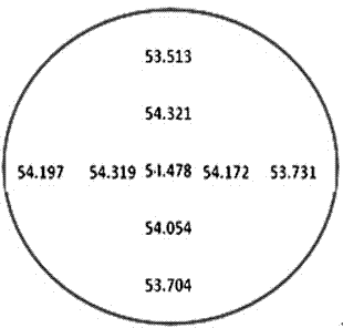
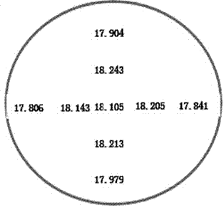
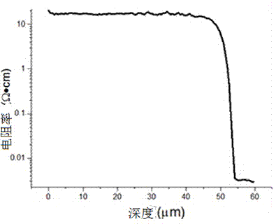

Image

  • Method for growing high-resistance thick layer silicon epitaxy on 6-inch heavily As-doped silicon substrate
  • Method for growing high-resistance thick layer silicon epitaxy on 6-inch heavily As-doped silicon substrate
  • Method for growing high-resistance thick layer silicon epitaxy on 6-inch heavily As-doped silicon substrate

Examples


Embodiment 1

[0029] (1) Use hydrogen chloride gas with a purity ≥ 99.99% to corrode the base of the epitaxial furnace at high temperature to completely remove the residual deposits on the base. The temperature is set at 1090°C, and the flow rate of hydrogen chloride gas is set at 5 L / min. The etching time was set to 10 min;

[0030] (2) Load the silicon substrate into the pit of the base of the epitaxial furnace, and use nitrogen and hydrogen with a purity of ≥99.999% to purge the cavity of the epitaxial furnace for 8 minutes in sequence, and set the gas flow rate to 100 L / min;

[0031] (3) Use hydrogen chloride gas to perform in-situ etching on the surface of the silicon substrate, which can polish the surface of the substrate and help to improve the lattice structure. Hydrogen gas is used to transport hydrogen chloride into the reaction chamber, and the hydrogen flow rate is set to 150 L / min, the hydrogen chloride flow rate is set to 2 L / min, the temperature is set to 1065°C, and the ti...

Embodiment 2

[0038](1) Use hydrogen chloride gas with a purity ≥ 99.99% to corrode the base of the epitaxial furnace at high temperature to completely remove the residual deposits on the base. The temperature is set at 1080°C, and the flow rate of hydrogen chloride gas is set at 5 L / min. The etching time was set to 10 min.

[0039] (2) Load the silicon substrate into the pit of the base of the epitaxial furnace, and use nitrogen and hydrogen with a purity of ≥99.999% to purge the cavity of the epitaxial furnace for 8 minutes in sequence, and set the gas flow rate to 150 L / min.

[0040] (3) Use hydrogen chloride gas to perform in-situ etching on the surface of the silicon substrate, which can polish the surface of the substrate and help to improve the lattice structure. Hydrogen gas is used to transport hydrogen chloride into the reaction chamber, and the hydrogen flow rate is set to 150 L / min, the hydrogen chloride flow rate is set to 2 L / min, the temperature is set to 1070°C, and the tim...

Embodiment 3

[0047] (1) Use hydrogen chloride gas with a purity ≥ 99.99% to corrode the base of the epitaxial furnace at high temperature to completely remove the residual deposits on the base. The temperature is set at 1080°C, and the flow rate of hydrogen chloride gas is set at 5 L / min. The etching time was set to 10 min.

[0048] (2) Load the silicon substrate into the pit of the base of the epitaxial furnace, and use nitrogen and hydrogen with a purity ≥99.999% to purge the cavity of the epitaxial furnace for 10 minutes in sequence, and set the gas flow rate to 150 L / min.

[0049] (3) Use hydrogen chloride gas to perform in-situ etching on the surface of the silicon substrate, which can polish the surface of the substrate and help to improve the lattice structure. Hydrogen gas is used to transport hydrogen chloride gas into the reaction chamber, and the hydrogen flow rate is set to 150 L / min, the hydrogen chloride flow rate is set to 1 L / min, the temperature is set to 1070°C, and the ...


PUM


Abstract

The invention relates to a method for growing a high-resistance thick layer silicon epitaxy on a 6-inch heavily As-doped silicon substrate. In the method, a normal-pressure flat plate type epitaxial furnace is adopted. The method comprises the following steps: (1) corroding an epitaxial furnace base by using hydrogen chloride with the purity of not less than 99.99 percent at a high temperature; (2) loading a silicon substrate sheet in the epitaxial furnace, purging a cavity of the epitaxial furnace for 8-10min by sequentially using nitrogen and hydrogen with purities of not less than 99.99 percent; (3) performing in-situ corrosion on the surface of the silicon substrate sheet by using hydrogen chloride gas; (4) purging the surface of the silicon substrate sheet by large-flow hydrogen; (5) growing an intrinsic epitaxial layer on the substrate by using non-doped trichlorosilane; (6) growing a doped epitaxial layer; and (7) cooling after the epitaxial layer reaches a preset temperature during growing. The method has the beneficial effects of being used for successfully preparing a high-resistance thick layer silicon epitaxy structure with thickness non-uniformity of less than 1 percent and specific resistance non-uniformity of less than 1 percent, without defects of a stacking fault, dislocation, a slip line and fog, with an optimal transition region width of less than 4 micrometers, good uniformity and a narrow transition region, and capable of completely meeting a requirement of a power MOS device on a silicon epitaxial material in an aspect of a parameter.

Description

technical field [0001] The invention relates to a semiconductor material preparation technology, in particular to a method for growing high-resistance thick-layer silicon epitaxy on a 6-inch heavy arsenic-doped substrate. Background technique [0002] High-resistance thick-layer silicon epitaxial wafers generally refer to epitaxial wafers with a thickness ranging from 30 to 150 μm and a resistivity greater than 15W×cm. This type of epitaxial wafer is mainly used for MOSFETs and power amplifier devices. As the diameter of silicon wafers continues to increase, it becomes more difficult to control the uniformity and defects within the wafer. High-resistance thick-layer silicon epitaxial wafers usually choose arsenic-doped and antimony-doped substrates, in which arsenic-doped (r: 0.002~0.004W×cm) silicon substrates are compared with antimony-doped (r: 0.01~0.02W×cm) The silicon substrate has a lower resistivity, which can reduce the forward conduction voltage drop when applied ...

Claims


Application Information

Patent Timeline
IPC IPC(8): H01L21/205
CPCH01L21/02532H01L29/78
Inventor 王文林高航薛兵李明达
Owner CHINA ELECTRONICS TECH GRP NO 46 RES INST
Why Eureka
Try Eureka