

Deposition method adopting combination of arc ion plating and high power pulsed magnetron sputtering
A magnetron sputtering compound and high-power pulse technology, which is applied in the field of material surface treatment, can solve the problems of low film deposition efficiency and unstable discharge, etc., and achieve the goal of ensuring high-density continuous generation, increasing energy, and compensating for the limitation of discharge instability. Effect
- Summary
- Abstract
- Description
- Claims
- Application Information
AI Technical Summary
Problems solved by technology
Method used
Image

Examples
specific Embodiment approach 1
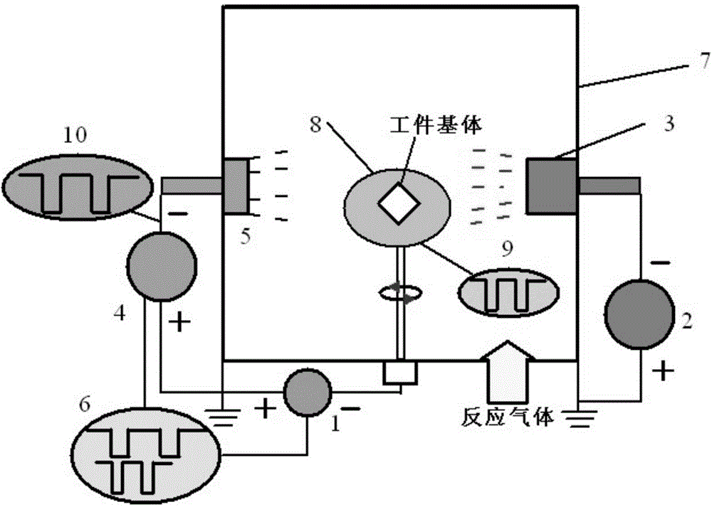
[0020] Specific implementation mode one: the following combination figure 1 and figure 2 Description of this embodiment, the device used in the composite deposition method of arc ion plating and high-power pulse magnetron sputtering in this embodiment includes bias power supply 1, arc power supply 2, arc ion plating target source 3, high-power pulse magnetron sputtering Power supply 4, high-power pulse magnetron sputtering target source 5, waveform synchronous matching device 6, vacuum chamber 7, sample stage 8, bias power waveform oscilloscope 9 and high-power pulse magnetron sputtering power waveform oscilloscope 10;
[0021] The method includes the following steps:
[0022] Step 1. Place the workpiece to be processed on the sample stage 7 in the vacuum chamber 7, connect the workpiece to the pulse output terminal of the bias power supply 1, and connect the magnetron sputtering target source 4 installed on the vacuum chamber 7 to the high-power pulse magnetron The high-po...
specific Embodiment approach 2
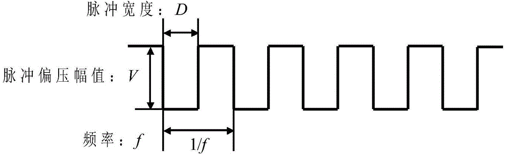
[0035] Specific embodiment two: the difference between this embodiment and embodiment one is that the device used in the method also includes a bias power waveform oscilloscope 8 and a high-power pulse magnetron sputtering power waveform oscilloscope 9, and a bias power waveform oscilloscope 8 It is used to display the voltage and current waveforms issued by the bias power supply 1, and the waveform oscilloscope 9 of the high-power pulse magnetron sputtering power supply is used to display the pulse voltage and current waveforms issued by the high-power pulse magnetron sputtering power supply 4. Others are the same as those in the embodiment same.
specific Embodiment approach 3
[0036] Specific implementation mode three: the following combination image 3 This embodiment is described. The difference between this embodiment and Embodiment 1 is that during coating, the bias power supply 1 is first turned on by the waveform synchronous matching device 6, and then the high-power pulse magnetron sputtering power supply 4 is turned on. Embodiment 1 is the same.
PUM
 Abstract
Description
Claims
Application Information