Forming method of CMOS image sensor transfer transistor

A transfer transistor and image sensor technology, applied in the field of image sensors, can solve the problems of poor negative pressure signal stability, large output signal noise, and increased process cost, etc., to reduce process cost, save area, and reduce dark current or white spots Effect

Pending Publication Date: 2022-01-14
GALAXYCORE SHANGHAI
View PDF0 Cites 0 Cited by
  • Summary
  • Abstract
  • Description
  • Claims
  • Application Information

AI Technical Summary

Problems solved by technology

In the analog circuit, the negative pressure signal needs to be realized through the "charge pump". This structure has the following two problems: the stability of the negative pressure signal generated by the "charge pump" is poor, and the signal and the signal in the floating diffusion area exist Coupling effect, so this structure will lead to larger output signal noise; "charge pump" needs to be realized through a large capacitor and an additional circuit structure, so it needs to occupy a larger area and increase the process cost

Method used


Image

  • Forming method of CMOS image sensor transfer transistor
  • Forming method of CMOS image sensor transfer transistor
  • Forming method of CMOS image sensor transfer transistor

Examples


Embodiment 1

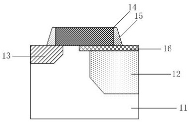
[0035] refer to figure 1 , the present embodiment provides a method for forming a transfer transistor of a CMOS image sensor, comprising: providing a substrate 11, forming a photodiode 12, a floating diffusion region 13, and forming at least one transfer transistor in the substrate 11;

[0036] P-type doped polysilicon 14 is correspondingly deposited on the photodiode 12 as the gate of the transfer transistor. When the charge accumulation state of the photodiode is applied, the voltage applied to the gate of the transfer transistor is greater than or equal to 0V.

[0037] Using p-type doped transfer transistor gate transfer transistor gate, when the photodiode is in the charge accumulation state, only need to apply a voltage of 0V or more to achieve the pinning effect, without the need to use large capacitors and additional circuit structures , save the area, reduce the process cost, and at the same time, the stability of the voltage signal is high.

[0038] The substrate 11 ...

Embodiment 2

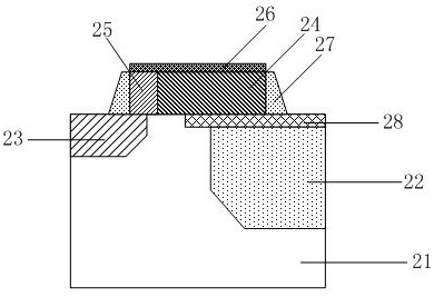
[0042] refer to figure 2 , the present embodiment provides a method for forming a transfer transistor of a CMOS image sensor, comprising: providing a semiconductor substrate 21, forming a photodiode 22, a floating diffusion region 23 and forming at least one transfer transistor in the substrate 21;

[0043] P-type doped polysilicon 24 is correspondingly deposited above the photodiode 22 as a part of the gate of the transfer transistor. When the charge accumulation state of the photodiode is applied, the voltage applied to the gate of the transfer transistor is greater than or equal to 0V.

[0044] The gate of the transfer transistor can be all p-type doped polysilicon, or partially p-type doped polysilicon. In this embodiment, the gate of the transfer transistor further includes n-type doped polysilicon 25 near the side of the floating diffusion region 23. When the charge accumulation state of the photodiode is applied, the voltage applied to the gate of the transfer transist...

Embodiment 3

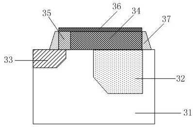
[0052] This embodiment provides a method for forming a transfer transistor of a CMOS image sensor. Its technical solution is similar to that of Embodiment 2. The difference from Embodiment 2 is that p-type doped polysilicon completely covers the carrier collection region of the photodiode. A pinning effect on the upper surface of the photodiode is achieved.

[0053] Specifically, refer to image 3 , providing a method for forming a CMOS image sensor transfer transistor, comprising: providing a semiconductor substrate 31, forming a photodiode 32, a floating diffusion region 33 and forming at least one transfer transistor in the substrate 31;

[0054] P-type doped polysilicon 34 is correspondingly deposited on the photodiode 32 as the gate or a part of the gate of the transfer transistor. When the charge accumulation state of the photodiode is applied, the voltage applied to the gate of the transfer transistor is greater than or equal to 0V.

[0055] In this embodiment, the p-t...


PUM


Abstract

The invention provides a forming method of a CMOS image sensor transfer transistor. The forming method comprises the following steps: forming a photodiode and a floating diffusion region; forming at least one transfer transistor; correspondingly depositing p-type doped polycrystalline silicon above the photodiode to serve as a transfer transistor grid electrode or a part of the grid electrode; and when the photodiode is in a charge accumulation state, determining that the voltage applied to the grid electrode of the transfer transistor is greater than or equal to 0V. When the p-type doped transfer transistor grid electrode is adopted and the photodiode is in a charge accumulation state, the pinning effect can be achieved only by applying a voltage of 0V or more than 0V, a large capacitor and an additional circuit structure do not need to be adopted, the area is saved, the process cost is reduced, and meanwhile the stability of a voltage signal is high.

Description

technical field [0001] The invention relates to the technical field of image sensors, in particular to a method for forming a transfer transistor of a CMOS image sensor. Background technique [0002] As a device unit that converts optical signals into digital electrical signals, CMOS image sensors are widely used in various emerging fields such as smartphones, tablet computers, automobiles, and medical care. As the core module of the image sensor, the pixel array is mainly composed of photodiodes, transfer transistors, reset transistors, and source follower transistors. Among them, the transfer transistor is located between the photodiode and the floating diffusion region to realize the switching function. The role of the floating diffusion region is to collect electrons converted by the photodiode, and convert the electronic signal into a corresponding voltage signal according to its conversion gain capability. [0003] In the prior art, the transfer transistor uses an n-t...

Claims


Application Information

Patent Timeline
IPC IPC(8): H01L27/146H01L21/28H01L21/336H01L29/06
CPCH01L27/14689H01L27/14692H01L29/66477H01L21/28008H01L29/0684
Inventor 李杰李玮
Owner GALAXYCORE SHANGHAI
Why Eureka
Try Eureka