Pixel circuit and display device

A pixel circuit and common electrode technology, which is applied in the field of display devices, can solve the problems of reducing the aperture ratio, complex peripheral drive circuits, and complex structures, and achieve the effect of reducing unevenness

Active Publication Date: 2015-08-26
PEKING UNIV SHENZHEN GRADUATE SCHOOL
View PDF5 Cites 57 Cited by
  • Summary
  • Abstract
  • Description
  • Claims
  • Application Information

AI Technical Summary

Problems solved by technology

However, the voltage-type pixel circuit cannot accurately compensate the drift of the threshold voltage, and it is difficult to compensate for the difference in mobility of different devices on the panel.
In addition, the voltage-ty

Method used


Image

  • Pixel circuit and display device
  • Pixel circuit and display device
  • Pixel circuit and display device

Examples


Embodiment 1

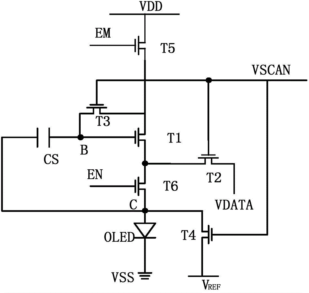
[0039] Please refer to figure 2 , figure 2 Shown is the structure of an embodiment of the pixel circuit of the present application, including: a storage capacitor CS, a third transistor T3, a second transistor T2, and a light-emitting branch for coupling between the first common electrode VDD and the second common electrode VSS road. The light emitting branch circuit includes a fifth transistor T5, a driving transistor T1, a sixth transistor T6 and a light emitting element OLED connected in series.

[0040]Wherein, the fifth transistor T5 is connected in series between the first common electrode VDD and the driving transistor T1, the sixth transistor T6 is connected in series between the second common electrode VSS and the driving transistor T1, and the control electrode (eg gate) of the fifth transistor T5 It is used to input the first control signal EM; the control pole (such as the gate) of the sixth transistor T6 is used to input the second control signal EN; the first...

Embodiment 2

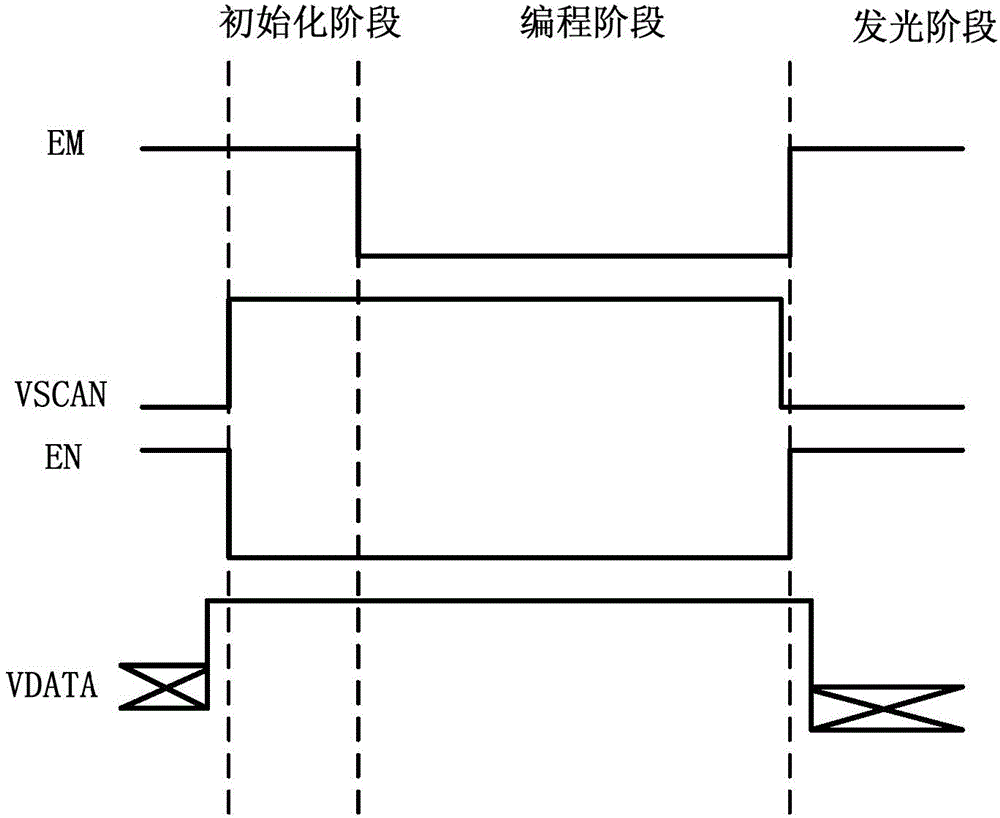
[0058] according to image 3 It can be seen that the phase of the second control signal EN is opposite to that of the scanning signal VSCAN, that is, when the second control signal EN is at a high level, the scanning signal VSCAN is at a low level; when the scanning signal VSCAN is at a high level, the second control signal EN is at a low level level. Based on this, this embodiment reduces the input of signal lines by changing the types of certain transistors. Please refer to Figure 4 , in the above embodiment, each transistor is an N-channel transistor, and in this embodiment, the sixth transistor T6 is selected as a P-channel transistor. At this time, the sixth transistor T6 and the second transistor T2 The channel types are different, and the second control signal EN is provided by the scan signal VSCAN. Please refer to Figure 5 , is the signal timing diagram of the pixel circuit in this embodiment, wherein the timing relationship between the scanning signal VSCAN and...

Embodiment 3

[0062] Please refer to Figure 6 , is the pixel circuit structure diagram of this embodiment. The difference between this embodiment and the above embodiment is that the positions of the light-emitting elements OLED in the light-emitting branch are connected in different positions, and the first end of the light-emitting element OLED in this embodiment is coupled to the first common electrode VDD, specifically:

[0063]The first terminal (such as the anode) of the light-emitting element OLED and the first pole (such as the drain) of the fourth transistor T4 are coupled to the first common electrode VDD; the second terminal (such as the cathode) of the light-emitting element OLED and the fourth transistor T4 The second pole (such as the source) is coupled to the first pole (such as the drain) of the fifth transistor T5; the control pole (such as the gate) of the fourth transistor T4 is used for input and responds to the scan signal VSCAN to switch on / off open state. Similarly...


PUM


Abstract

The application discloses a pixel circuit and a display device. The pixel circuit comprises a storage capacitor, a third transistor, a second transistor and a light-emitting branch used for connecting in series between a first common electrode and a second common electrode, and the light-emitting branch comprises a fifth transistor, a driving transistor, a sixth transistor and a light-emitting element which are connected in series. In an initialization stage, the third transistor and the fifth transistor conduct and initialize the potentials at the two ends of the storage capacitor, in a programming stage, the second transistor inputs a data signal to one end of the storage capacitor via the third transistor and stores, and in an luminescence stage, the driving transistor drives the light-emitting element to emit light according to the voltage difference at the two ends of the storage capacitor. By the pixel circuit and the display device, the threshold voltage of the driving transistor and the degeneration of the light-emitting element can be compensated, at the same time, the contrast of a display also can be increased.

Description

technical field [0001] The present application relates to a display device, in particular to a pixel circuit and a display device. Background technique [0002] Organic Light-Emitting Diode (OLED) display has been extensively studied in recent years due to its advantages of high brightness, high luminous efficiency, wide viewing angle and low power consumption, and has been rapidly applied to a new generation of displays. There are two driving modes for OLED display: passive matrix driving (Passive Matrix OLED, PMOLED) and active matrix driving (Active Matrix OLED, AMOLED). Although the cost of passive matrix driving is low, it cannot realize high-resolution display due to crosstalk phenomenon, and the passive matrix driving current is large, which reduces the service life of OLED. In contrast, the active matrix driving method sets a different number of transistors on each pixel as a current source, which avoids crosstalk, requires less driving current, and lower power cons...

Claims


Application Information

Patent Timeline
IPC IPC(8): G09G3/32
Inventor 张盛东王翠翠冷传利
Owner PEKING UNIV SHENZHEN GRADUATE SCHOOL
Why Eureka
Try Eureka