Packaging structure and packaging technology improving optical coupler reliability

A reliability and optocoupler technology, which is applied in the direction of semiconductor/solid-state device parts, semiconductor devices, electrical components, etc., can solve the problems of increasing manufacturing costs, reducing product reliability, reducing the reliability of gold wire welding, etc. Effects of production cost, increase of soldering temperature and reduction of production difficulty

Active Publication Date: 2015-08-26
NINGBO QUNXIN MICRO-ELECTRONICS CO LTD
View PDF4 Cites 3 Cited by
  • Summary
  • Abstract
  • Description
  • Claims
  • Application Information

AI Technical Summary

Problems solved by technology

However, there are also disadvantages in adopting this structure: the silica gel expands when it is heated (170-180°C) during molding, and shrinks after cooling after molding. Reduced product reliability issues
[0006] In summary, the improved optocoupler packaging structure and packaging process, although the soldering temperature is increased, can make the optocoupler apply the SMT chip soldering process in the soldering process; however, the silicone surface treatment process is complicated and the manufacturing cost is greatly increased. defects, and the stress of silicone between the molding material and the chip and the gold wire will reduce the reliability of the gold wire soldering

Method used


Image

  • Packaging structure and packaging technology improving optical coupler reliability
  • Packaging structure and packaging technology improving optical coupler reliability
  • Packaging structure and packaging technology improving optical coupler reliability

Examples


Embodiment Construction

[0023] In order to make the technical problems, technical solutions and beneficial effects to be solved by the present invention clearer, the present invention will be described in detail below in conjunction with the accompanying drawings and embodiments. It should be noted that the specific embodiments described here are only used to explain the present invention, not to limit the present invention.

[0024] The packaging process for improving the reliability of the optocoupler specifically includes the following steps:

[0025] first step. Coupling and alignment

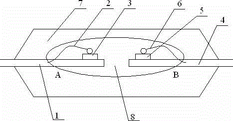
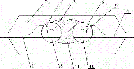
[0026] The input-end chip 3 and the output-end chip 5 of the optocoupler are bonded on the input-end frame 1 and the output-end frame 4 respectively by using conductive paste, and the input-end frame and the output-end frame are placed side by side in the housing.

[0027] The second step. welding

[0028] Solder the gold wires on the input chip and the output chip respectively.

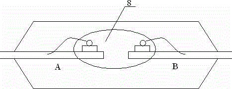
[0029] third step. Encapsul...


PUM


Abstract

The invention discloses a packaging structure and a packaging technology improving optical coupler reliability; the packaging technology specifically comprises the following steps: coupling, aligning and racking; packing an input end and an output end; setting a high voltage block layer; and mould pressing. The high voltage block layer is arranged between an input end transparent silica gel layer and an output end transparent silica gel layer; a mould pressing material is filled between the input end transparent silica gel layer and the output end transparent silica gel layer, and between an outer wall of the high voltage block layer and a housing. The packaging technology can improve a soldering temperature, so SMT paster soldering technology can be applied to an optical coupler welding process; a stress between a chip welding gold thread and the silica gel and mould pressing material and a high voltage breakdown path in the optical coupler can be removed without needing a silica gel surface treatment complex technology condition, thus reducing production difficulty and production cost, and effectively ensuring product reliability.

Description

technical field [0001] The invention relates to the technical field of electronic components, in particular to a packaging process for improving the high-voltage performance of an optocoupler. Background technique [0002] Optocoupler is the abbreviation of optocoupler and photoelectric isolator. It uses light as the medium to transmit electrical signals. It has a good isolation effect on input electrical signals and output electrical signals. It has strong anti-interference ability, stable operation, no contact, and long service life. Long, high transmission efficiency, so widely used in the circuit. [0003] The packaging structure of ordinary optocouplers is as follows: figure 1 As shown, the input chip 3 and the output chip 5 are included, the input chip and the output chip are respectively arranged on the input frame 1 and the output frame 4, and gold wires are welded on the input chip and the output chip; In the packaging process of ordinary optocouplers, the input c...

Claims


Application Information

Patent Timeline
Patent Type & Authority Applications(China)
IPC IPC(8): H01L25/16H01L23/31H01L21/56H01L21/50
CPCH01L2224/45144H01L2224/48091H01L2224/48465H01L2924/00014H01L2924/00
Inventor 沈震强
Owner NINGBO QUNXIN MICRO-ELECTRONICS CO LTD
Why Eureka
Try Eureka