Concentrating Photoelectric Conversion Device And Manufacturing Method Thereof

A technology of photoelectric conversion device and manufacturing method, which is applied in photovoltaic power generation, final product manufacturing, sustainable manufacturing/processing, etc., and can solve problems such as inability to obtain power generation

Active Publication Date: 2015-08-26
SHIN ETSU CHEM IND CO LTD
View PDF6 Cites 1 Cited by
  • Summary
  • Abstract
  • Description
  • Claims
  • Application Information

AI Technical Summary

Problems solved by technology

[0003] However, conventional concentrating photoelectric conversion devices have the following problems: On sunny days, compared with flat-panel sola

Method used


Image

  • Concentrating Photoelectric Conversion Device And Manufacturing Method Thereof
  • Concentrating Photoelectric Conversion Device And Manufacturing Method Thereof
  • Concentrating Photoelectric Conversion Device And Manufacturing Method Thereof

Examples


Embodiment 1

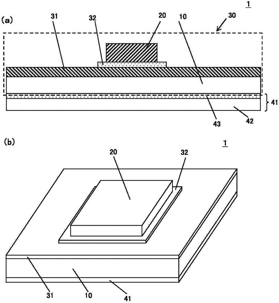
[0199] First, the silicon solar cell 10' is mounted on the external connection substrate 41, ie, the PCB substrate, using solder paste, and then UV ozone treatment is performed.

[0200] Next, using a vacuum laminator (manufactured by Nichigo-Morton Co., Ltd.), a film-coated silicone resin (AF-500 (model number): manufactured by Shin-Etsu Chemical Co., Ltd.) The insulating layer 31 is made by pasting on the surface of the silicon solar cell 10'.

[0201] Next, silver paste (manufactured by Shin-Etsu Chemical Co., Ltd.) was screen-printed on the insulating layer 31 to prepare the electrode layer 32 on which the group III-V multi-junction solar cell 20' for concentrating solar cells was placed.

[0202] After forming the electrode layer, a III-V multi-junction solar cell 20', which is a concentrating solar cell, is mounted using lead-free solder.

[0203] Next, the photoelectric conversion element 30 mounted on the external connection substrate 41 is arranged in a mold, and sil...

Embodiment 2

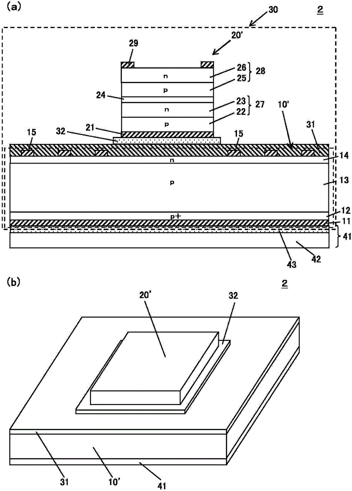
[0205] First, the silicon solar cell 10' is mounted on the external connection substrate 41, ie, the PCB substrate, using solder paste, and then UV ozone treatment is performed.

[0206] Next, using a vacuum laminator (manufactured by Nichigo-Morton Co., Ltd.), a film made by mixing silicone resin (AF-500 (model): Shin-Etsu Chemical Co., Ltd.) and phosphor is attached to the silicon solar cell 10'. On the surface, an insulating layer 31 of 50 μm was formed.

[0207] Next, silver paste is screen-printed on the insulating layer 31 to prepare the electrode layer 32 on which the III-V multi-junction solar cell 20', which is the concentrating solar cell, is mounted.

[0208] After forming the electrode layer, a III-V multi-junction solar cell 20', which is a concentrating solar cell, is mounted using lead-free solder.

[0209] Next, the photoelectric conversion element 30 connected to the external connection substrate 41 is arranged in a mold, and silicone resin (LPS-3541 (model):...


PUM

PropertyMeasurementUnit
Thicknessaaaaaaaaaa

Abstract

The present invention aims to provide a concentrating photoelectric conversion device which does not need to carry out the band gap design again, and can easily manufacture a solar cell which also can be obtained by the non-solar cell manufacturers, is easy in heat radiation design, and can restrain the reduction of the conversion efficiency even improving the concentrating multiplying power. The concentrating photoelectric conversion device provided by the present invention is equipped with a concentrating lens and a photoelectric conversion element arranged at the position opposite to the concentrating lens, and is characterized in that the photoelectric conversion element is equipped with a scattered light solar cell, an insulating layer arranged on the concentrating lens side surface of the scattered light solar cell, an electrode layer arranged on the insulating layer and a concentrating solar cell arranged on the electrode layer and electrically connected with the electrode layer. Moreover, the concentrating lens is made of a transparent heat convertible resin, the photoelectric conversion element is carried on an external connecting substrate, and the scattered light solar cell and the concentrating solar cell are separated electrically.

Description

technical field [0001] The invention relates to a concentrating photoelectric conversion device and a manufacturing method thereof. Background technique [0002] Conventionally, as a photoelectric conversion device, a solar power generation device that converts solar energy into electrical energy has been put into practical use. The condenser mirror irradiates collected sunlight to a solar cell element having a smaller light-receiving area than the condenser mirror to obtain electrical energy (for example, refer to Patent Document 1). [0003] However, conventional concentrating photoelectric conversion devices have the following problems: On sunny days, compared with flat-panel solar cell modules (modules) using ordinary silicon solar cells, more power can be obtained, but almost no power can be obtained on cloudy days. quantity. [0004] In order to solve the above-mentioned problems, a concentrating photoelectric conversion device has been proposed, which has a structur...

Claims


Application Information

Patent Timeline
IPC IPC(8): H01L31/0725H01L31/054H01L31/052H01L31/18
CPCY02E10/52Y02E10/544Y02E10/549Y02P70/50
Inventor 后藤涉塩原利夫
Owner SHIN ETSU CHEM IND CO LTD
Why Eureka
Try Eureka