Method for manufacturing organic light emitting display device

A light-emitting display, organic technology, applied in semiconductor/solid-state device manufacturing, electrical components, circuits, etc.

Active Publication Date: 2015-08-26
DONGWOO FINE CHEM CO LTD
View PDF7 Cites 9 Cited by
  • Summary
  • Abstract
  • Description
  • Claims
  • Application Information

AI Technical Summary

Problems solved by technology

However, this patent does not fundamentally solve the above-mentioned problems

Method used


Image

  • Method for manufacturing organic light emitting display device
  • Method for manufacturing organic light emitting display device

Examples


Embodiment

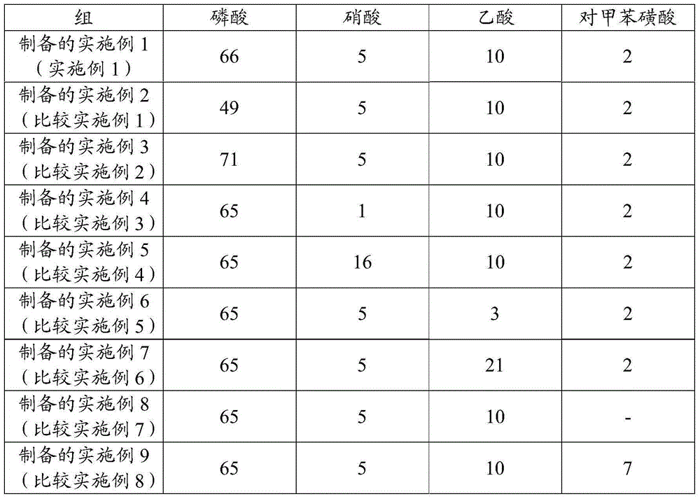
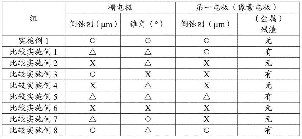
[0078] Examples and Comparative Examples

[0079] (1) Preparation of etchant composition

[0080] Etchant compositions having various constituent components and contents listed in Table 1 below and including the balance of water were prepared.

[0081] [Table 1]

[0082]

[0083] (2) Formation of metal wires

[0084] 1) Gate electrode

[0085] A Mo / Al / Mo metal layer is formed on a glass substrate by a deposition method, and the formed layer metal layer is etched using each of the above-mentioned etchant compositions to form a gate electrode.

[0086] 2) The first electrode

[0087] A gate electrode, a source electrode, and a drain electrode are formed on the glass substrate, and then a passivation layer is formed on the glass substrate. Thereafter, a laminated layer structure of ITO / APC(AgPdCu) / ITO was formed on the passivation layer, and then etched using the respective etchant compositions described above to form the first electrode. Here, the drain electrode and the ...


PUM

PropertyMeasurementUnit
electrical resistivityaaaaaaaaaa

Abstract

The present invention discloses a method for manufacturing an organic light emitting display device, comprising the steps of: a) forming a gate electrode on a substrate; b) forming a gate insulating layer on the substrate comprising the gate electrode; c) forming an active layer on the gate insulating layer; d) forming an insulating layer on the active layer; e) forming a source electrode and a drain electrode contacted with the active layer on the insulating layer; f) forming a passivation layer on the insulating layer for covering the source electrode and the drain electrode; and g) forming an organic light emitting element electrically connected with one of the source electrode and the drain electrode, wherein the step a) comprises forming a metal layer or a laminating layer of aluminum, molybdenum, or silver, and etching the metal layer to form the gate electrode through an etching agent composition, wherein the etching agent composition comprises 50%-70% by weight of phosphoric acid, 2%-15% by weight of nitric acid, 5%-20% by weight of acetic acid, 0.1%-5% by weight of para-toluenesulfonic acid, and the balance water, in this way, metal layers of the gate electrode and a pixel electrode can be etched at the same time, thus excellent etching effect can be achieved, and the organic light emitting display device can be manufactured with improved process efficiency.

Description

technical field [0001] The invention relates to a method for manufacturing an organic light emitting display device. Background technique [0002] In general, flat panel display devices can be classified into light emitting type devices and light receiving type devices. Light emitting devices may include, for example, cathode ray tubes, plasma display panels, electroluminescent devices, light emitting diodes, and the like. The light-receiving type device may include, for example, a liquid crystal display. Among these, the electroluminescent device has several advantages such as a wide viewing angle, excellent contrast ratio, and high response speed, and thus, it has attracted public attention as a next-generation display device. [0003] Such electroluminescent devices are classified into inorganic electroluminescent devices and organic electroluminescent devices according to the material forming the light emitting layer. [0004] Among these, the organic electroluminesce...

Claims


Application Information

Patent Timeline
Patent Type & Authority Applications(China)
IPC IPC(8): H01L51/56H01L27/32
CPCH10K99/00H10K71/60H10K59/12H10K71/00H01L29/4908H01L21/32134C23F1/16
Inventor 张尚勋金泰完沈庆辅
Owner DONGWOO FINE CHEM CO LTD
Why Eureka
Try Eureka