Novel organic compound and organic light emitting device containing same
A technology of organic compounds and compounds, applied in the fields of organic chemistry, electrical components, light-emitting materials, etc., can solve the problems of high driving voltage, short service life, practical difficulties, etc., and achieve low driving voltage, long service life, high triplet state energy effect
- Summary
- Abstract
- Description
- Claims
- Application Information
AI Technical Summary
Problems solved by technology
Method used
Image
Examples
Embodiment 1
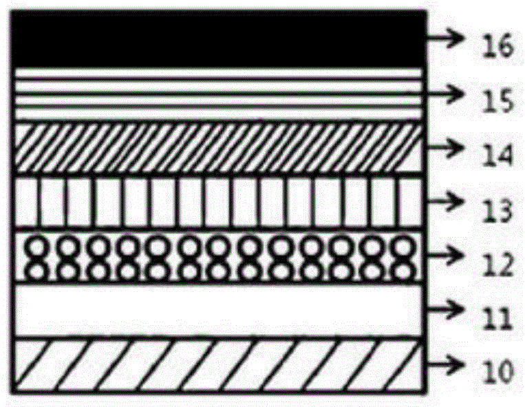
[0273] Ultrasonic cleaning with distilled water has a thickness of Indium Tin Oxide (ITO) thin film glass substrate. After cleaning with distilled water, use solvents such as isopropanol, acetone, and methanol to perform ultrasonic cleaning and dry, then transport to a plasma cleaner and use oxygen plasma to clean the above-mentioned substrate for 5 minutes, and then use thermal vacuum evaporation The thermal evaporator made a thickness of The film of compound 1 was used as a hole injection layer and a hole transport layer. Next, MADN (2-methyl-9,10-bis(naphthalene-2-yl)anthracene): BD01 (1,6-bis(N,Ndiphenylamino)pyrene) was used as the above-mentioned light-emitting layer at 5% doped to produce a thickness of membrane. Next, fabricated as an electron transport layer with a thickness of Alq 3 (Three (8-hydroxyquinoline) aluminum) film, the production thickness is The LiF film and the thickness is An aluminum (Al) film was used to seal (Encapsulate) the element in...
Embodiment 2 to Embodiment 17
[0275] An organic light-emitting device was prepared in the same manner as in Example 1, wherein Compound 2 to Compound 17 were used instead of Compound 1 in the hole injection layer and the hole transport layer, respectively, thereby producing an organic light-emitting device.
Embodiment 18
[0277] Ultrasonic cleaning with distilled water has a thickness of Indium Tin Oxide (ITO) thin film glass substrate. After cleaning with distilled water, use solvents such as isopropanol, acetone, and methanol to perform ultrasonic cleaning and dry, then transport to a plasma cleaner and use oxygen plasma to clean the above-mentioned substrate for 5 minutes, and then use thermal vacuum evaporation The thermal evaporator made a hole injection layer on the top of the ITO substrate with a thickness of The 2-TNATA (4,4',4"-tris[2-naphthylphenylamino]triphenylamine) film and the thickness of the hole transport layer are A film of compound 18 synthesized above. Next, CBP (4,4'-bis(N-carbazole)-1,1'-biphenyl):Ir(ppy) 3 doped at 7% while producing a thickness of membrane. Next, fabricated as an electron transport layer with a thickness of After the TPBi (1,3,5-tris(1-phenyl-1H-benzimidazol-2-yl)benzene) film, the thickness is The LiF film and the thickness is An aluminu...
PUM
| Property | Measurement | Unit |
|---|---|---|
| thickness | aaaaa | aaaaa |
Abstract
Description
Claims
Application Information


