


Quick Research
Generate reliable direction feasibility study reports for your R&D in just a few steps.

Technical Q&A
Discover and master advanced knowledge NOW. Basics, ideas, possibilities, all at once.

Find Solutions
As an expert in R&D theories, this can generate solutions to your technical problems instantly.

Evaluate Feasibility
Analyze your overall solution with one click, know your potential R&D risks in advance.

Monitor Landscape
Get weekly tech updates, stay abreast of the latest tech innovations and key insights.
Method for manufacturing crystal semiconductor film
A manufacturing method and semiconductor technology, applied in the direction of semiconductor/solid-state device manufacturing, semiconductor devices, transistors, etc., can solve the problems of uneven crystallinity, component differences, etc., and achieve the effect of reducing the difference in transistor characteristics and effective laser annealing treatment
- Summary
- Abstract
- Description
- Claims
- Application Information
AI Technical Summary
Problems solved by technology
Method used
Image

Examples
Embodiment 1
[0059] One embodiment of the present invention is described below.
[0060] Using 50 nm-thick amorphous Si as a non-single crystal semiconductor film, pulsed laser irradiation was performed by changing the number of times of irradiation under the following conditions.
[0061] Excimer laser: LSX315C / wavelength 308nm, frequency 300Hz
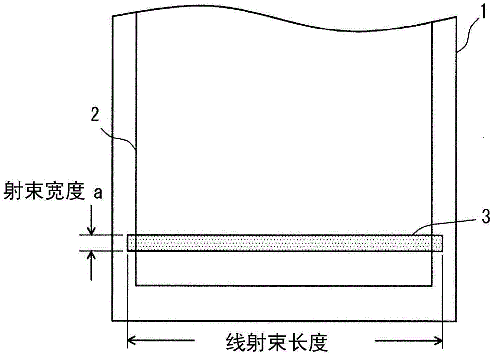
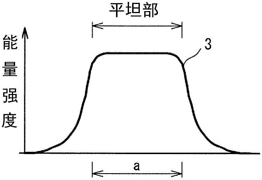
[0062] Beam size: beam length 500mm × beam width 0.16mm
[0063] The beam width is the flat portion in the high-intensity region where the maximum energy intensity is 96% or more
[0064] Scanning pitch: 40μm~80μm
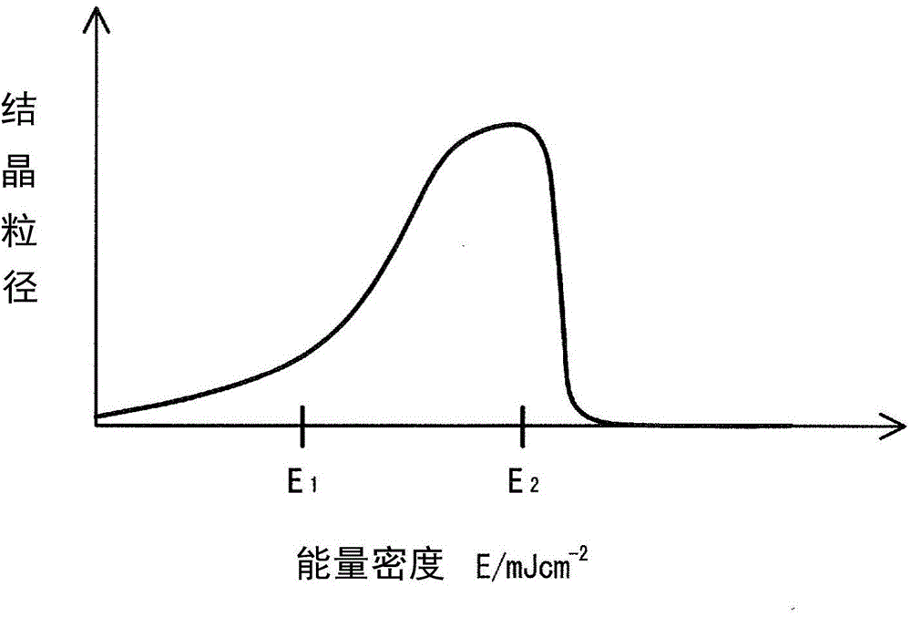
[0065] Irradiation pulse energy density: 370mJ / cm 2
[0066] Channel length: 20μm
[0067] The irradiation pulse energy density of the above-mentioned pulsed laser is below the irradiation pulse energy density capable of producing microcrystals, and within the range of irradiation times from four times to eight times, the crystal grain size gradually grows, and when the number of times of irradiation exceeds eight times When , t...
PUM
 Abstract
Description
Claims
Application Information
 - R&D Engineer
- R&D Manager
- IP Professional
- Industry Leading Data Capabilities
- Powerful AI technology
- Patent DNA Extraction
Browse by: Latest US Patents, China's latest patents, Technical Efficacy Thesaurus, Application Domain, Technology Topic, Popular Technical Reports.
© 2024 PatSnap. All rights reserved.Legal|Privacy policy|Modern Slavery Act Transparency Statement|Sitemap|About US| Contact US: help@patsnap.com