LED structure and formation method thereof
A technology of LED structure and nitride semiconductor, applied in semiconductor devices, electrical components, circuits, etc., can solve problems such as low luminous efficiency, and achieve the effects of improving luminous efficiency, reducing resistivity, and uniform diffusion
- Summary
- Abstract
- Description
- Claims
- Application Information
AI Technical Summary
Problems solved by technology
Method used
Image

Examples
Embodiment Construction
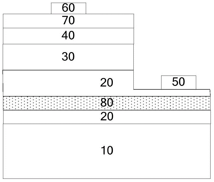
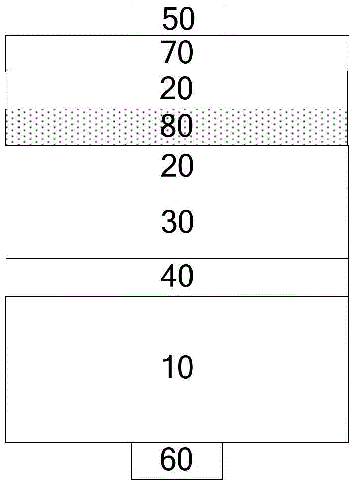
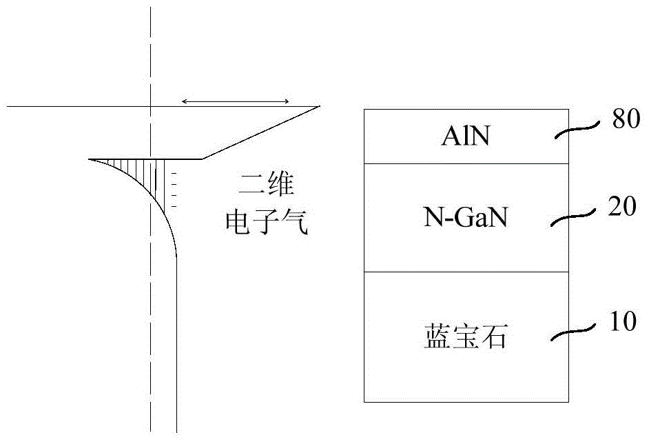
[0017] Embodiments of the present invention are described in detail below, examples of which are shown in the drawings, wherein the same or similar reference numerals designate the same or similar elements or elements having the same or similar functions throughout. The embodiments described below by referring to the figures are exemplary and are intended to explain the present invention and should not be construed as limiting the present invention.
[0018] In describing the present invention, it should be understood that the terms "center", "longitudinal", "transverse", "length", "width", "thickness", "upper", "lower", "front", " Orientation or position indicated by "back", "left", "right", "vertical", "horizontal", "top", "bottom", "inner", "outer", "clockwise", "counterclockwise", etc. The relationship is based on the orientation or positional relationship shown in the drawings, and is only for the convenience of describing the present invention and simplifying the descrip...
PUM
| Property | Measurement | Unit |
|---|---|---|
| Thickness | aaaaa | aaaaa |
Abstract
Description
Claims
Application Information
 - Generate Ideas
- Intellectual Property
- Life Sciences
- Materials
- Tech Scout
- Unparalleled Data Quality
- Higher Quality Content
- 60% Fewer Hallucinations
Browse by: Latest US Patents, China's latest patents, Technical Efficacy Thesaurus, Application Domain, Technology Topic, Popular Technical Reports.
© 2025 PatSnap. All rights reserved.Legal|Privacy policy|Modern Slavery Act Transparency Statement|Sitemap|About US| Contact US: help@patsnap.com