Self-powered micro-fluidic chip and manufacturing method thereof

A microfluidic chip, self-powered technology, applied in chemical instruments and methods, piezoelectric effect/electrostrictive or magnetostrictive motors, electrical components, etc., to achieve the effect of broad application prospects

Active Publication Date: 2015-09-23
HUBEI UNIV
View PDF6 Cites 19 Cited by
  • Summary
  • Abstract
  • Description
  • Claims
  • Application Information

AI Technical Summary

Problems solved by technology

This idea and practice of using piezoelectric materials to generate electricity in microfluidic chips has not been found in published literature or patented technologies

Method used


Image

  • Self-powered micro-fluidic chip and manufacturing method thereof
  • Self-powered micro-fluidic chip and manufacturing method thereof
  • Self-powered micro-fluidic chip and manufacturing method thereof

Examples


Embodiment 1

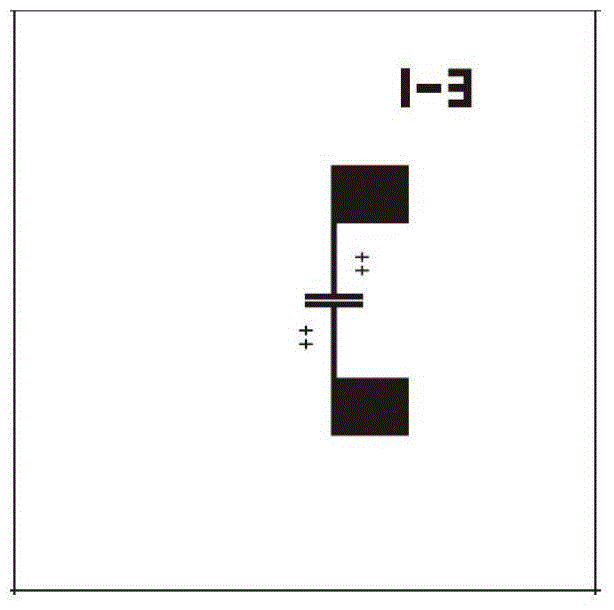
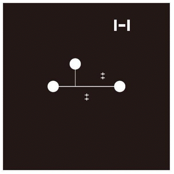
[0046] figure 2 It is a schematic diagram of the mask plate used for the electrode. The length of the electrode is 3 mm, the distance between the electrodes is 100 μm, and the overall size of the mask plate is 30 mm in length and width. image 3 It is a schematic diagram of the mask plate used for microfluidic channels. In the figure, the width of the main flow channel is b=100μm, the width of the branch channel is a=50μm, and the overall size of the mask plate is 30mm in length and width; the main flow channel and the branch flow channel of the liquid The angle between them is 90 degrees.

[0047] 1. Detection electrode preparation

[0048] (1) Substrate cleaning: Put the quartz glass sheet with a length and width of 20 mm and a thickness of 2 mm into acetone, alcohol, and deionized water in sequence, and ultrasonically clean it for 10 minutes at room temperature. After ultrasonic cleaning, pour out the last deionized water. Add new deionized water.

[0049] (2) Photolith...

Embodiment 2

[0076] refer to figure 2 , image 3 , in the mask plate used as the electrode, the length of the electrode is 3mm, the distance between the electrodes is 100 μm, and the overall size of the mask plate is 30mm in length and width. For the mask plate used for the microfluidic channel, the width of the main flow channel is b=200 μm, the width of the branch channel is a=50 μm, and the overall size of the mask plate is 30 mm in length and width; the angle between the main flow channel and the branch flow channel of the liquid is 90 degrees.

[0077] 1. Detection electrode preparation

[0078] (1) Substrate cleaning: Put the quartz glass sheet with a length and width of 20 mm and a thickness of 2 mm into acetone, alcohol, and deionized water in sequence, and ultrasonically clean it for 10 minutes at room temperature. After ultrasonic cleaning, pour out the last deionized water. Add new deionized water.

[0079] (2) Photolithography process: Take the cleaned quartz glass sheet a...

Embodiment 3

[0106] refer to figure 2 , image 3 , in the mask plate used as the electrode, the length of the electrode is 3 mm, the distance between the electrodes is 200 μm, and the overall size of the mask plate is 30 mm in length and width. The mask plate used for the microfluidic channel, the width of the main flow channel is b=300μm, the width of the branch channel is a=50μm, the overall size of the mask plate is 30mm in length and width; the angle between the main flow channel and the inlet branch channel is 90 degrees.

[0107] 1. Detection electrode preparation

[0108] (1) Substrate cleaning: Put the quartz glass sheet with a length and width of 20 mm and a thickness of 2 mm into acetone, alcohol, and deionized water in sequence, and ultrasonically clean it for 10 minutes at room temperature. After ultrasonic cleaning, pour out the last deionized water. Add new deionized water.

[0109] (2) Photolithography process: Take the cleaned quartz glass sheet and dry it with nitroge...


PUM


Abstract

The invention discloses a self-powered micro-fluidic chip and a manufacturing method thereof. A piezoelectric one-dimensional nano-material is utilized to collect tiny mechanical energy in the environment and convert the tiny mechanical energy into electric energy, and the electric potential energy is output to a sensitive unit so as to build the self-powered micro-fluidic chip. The micro-fluidic chip is divided into four layers, the undermost layer is a quartz glass substrate, a layer of exploring electrode is arranged on the quartz glass substrate, a layer of KNN nanofibers is arranged on the exploring electrode, and the uppermost layer is a PDMS cover plate with a PDMS microchannel. The manufacturing method of the self-powered micro-fluidic chip comprises the following steps: photo-etching, sputtering and stripping a substrate to produce an exploring electrode, adopting the electrospinning method to prepare potassium sodium niobate nanofibers in a large area on the exploring electrode, and then performing bonding on a PDMS microchannel and the substrate.

Description

technical field [0001] The invention relates to a microfluidic chip with a self-powered function and a manufacturing method thereof, in particular to a method for manufacturing a self-powered microfluidic chip based on the piezoelectric power generation effect, and belongs to the technical field of inorganic nano functional materials and microfluidics . Background technique [0002] Microfluidic technology is also called lab-on-a-chip. Using this technology, the basic operations involved in the field of biochemistry, such as sample preparation, reaction, separation and detection, can be integrated on a chip of a few square centimeters or even smaller. Compared with traditional analysis and testing platforms, the advantages of microfluidic chips lie in the integration of functions, low consumption of detection samples, and rapid sample detection. The electrical transport properties of semiconductor nanowires are very sensitive to biomolecules and heavy metal ions, which can...

Claims


Application Information

Patent Timeline
Patent Type & Authority Applications(China)
IPC IPC(8): B01L3/00H02N2/18
Inventor 顾豪爽潘绪敏王钊胡永明
Owner HUBEI UNIV
Why Eureka
Try Eureka