
Eutectic chip soldering method

A eutectic welding and chip technology, which is applied in the manufacture of electrical components, electrical solid devices, semiconductor/solid devices, etc., can solve problems such as scratches on the aluminum layer, great influence on welding quality, and failure to meet the surface quality of chips, etc., to achieve guaranteed Surface quality, the effect of simplifying the welding operation process

Inactive Publication Date: 2015-09-23
EAST CHINA INST OF OPTOELECTRONICS INTEGRATEDDEVICE
View PDF6 Cites 11 Cited by
  • Summary
  • Abstract
  • Description
  • Claims
  • Application Information

AI Technical Summary

Problems solved by technology

However, when using a vacuum controllable atmosphere eutectic furnace for welding, the vacuum degree is generally "5Pa ~ 10Pa". Under this condition, whether the pressure applied on the chip is appropriate has a great impact on the welding quality. Specially designed positioning fixture and matching pressurizing device, usually a pressurizing device is made on the heated metal or graphite fixture to realize the pressurization of the chip. In order to ensure the pressure, the pressurizing device generally uses a certain quality of metal compact, but Because the aluminum layer on the surface of the chip is very fragile, the roughness of the surface of the metal compact workpiece is enough to cause scratches on the aluminum layer on the surface of the chip, which cannot meet the requirements for ensuring the quality of the chip surface during welding

Method used


Image

  • Eutectic chip soldering method

Examples


Embodiment Construction

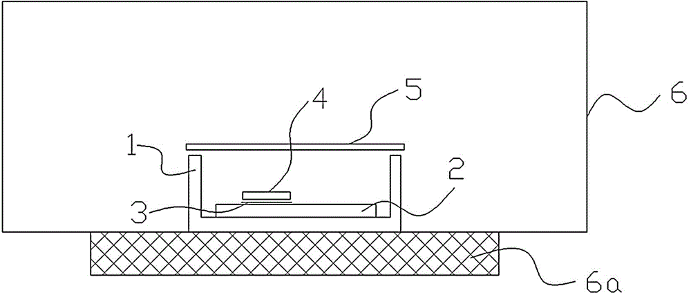
[0017] like figure 1 As shown, the present invention provides a chip eutectic welding method, comprising the following steps:

[0018] a) Clean the welding piece 3 and the part to be welded 2 (such as a ceramic substrate), remove the dirt on the surface of the welding piece 3 and the part to be welded 2, and perform surface grinding and ultrasonic cleaning on the welding piece 3 and the part to be welded 2 to achieve removal the purpose of defilement;

[0019] b) Cutting the welding piece 3 so that the size of the welding piece 3 is compatible with the chip 4, and performing a leveling operation on the welding piece 3, the area of ​​the welding piece 3 should be slightly larger than the area of ​​the chip 4;

[0020] c) placing the part to be welded 2 horizontally on the bottom of the metal container 1;

[0021] d) Put the welding piece 3 horizontally on the welding area of ​​the piece to be welded 2, and then place the chip 4 horizontally on the center of the welding piece ...


PUM


Abstract

The invention discloses an eutectic chip soldering method. The method comprises the steps that dirt at the surfaces of a soldering lug and a piece to be soldered is removed, the soldering lug is cut, the piece to be soldered, the soldering lug and a chip are placed in a metal container, the metal container is placed in an atmosphere controllable eutectic furnace, the temperature curve of the atmosphere controllable eutectic furnace is set according to technical requirements, eutectic soldering is carried out on the piece to be soldered and the chip, air in the atmosphere controllable eutectic furnace is exhausted before temperature rise, nitrogen of the flow of 2L / min is filled in the temperature rise process, it is ensured that the soldering lug is fused, the vacuum degree in the furnace in the temperature decrease process is lower than or equivalent to 1 Pa and kept for 30 to 60s, so that gas in the chip and the piece to be soldered and gas generated by fusing of the soldering lug can be smoothly extracted under the self-gravity of the chip and the high-vacuum condition, and thus, the chip is soldered with the piece to be soldered via the pressure of self gravity on the piece to be soldered instead of using additional pressuring device. Thus, the surface quality of the chip during soldering is ensured, and the soldering process is simplified.

Description

technical field [0001] The invention relates to the field of chip welding, in particular to a chip eutectic welding method. Background technique [0002] As we all know, with the development of hybrid integrated circuits towards high performance, high reliability, miniaturization, high uniformity and low cost, higher and higher requirements are put forward for the chip welding process. (such as substrates, shells, etc.) for interconnection, the main methods are conductive adhesive bonding and eutectic welding. Eutectic welding, also known as low melting point alloy welding, refers to the phenomenon of eutectic fusion of eutectic solder at relatively low temperatures. The eutectic alloy directly changes from solid to liquid without going through the plastic stage. Eutectic welding Due to the advantages of small resistivity, small thermal conductivity, small thermal resistance, low loss, and high reliability, it is widely used in chip bonding with high soldering process requi...

Claims


Application Information

Patent Timeline
IPC IPC(8): H01L21/58
CPCH01L24/83H01L2224/8309
Inventor 李寿胜夏俊生张剑邹建安臧子昂
Owner EAST CHINA INST OF OPTOELECTRONICS INTEGRATEDDEVICE
Learn More