Organic thin-film memory doped with carbon nano tubes

A technology of organic thin films and carbon nanotubes, applied in the field of microelectronics, can solve problems such as low efficiency and difficulty in obtaining good contact, achieve high performance, reduce production difficulty and production costs

Inactive Publication Date: 2015-09-23
FUDAN UNIV
View PDF5 Cites 3 Cited by
  • Summary
  • Abstract
  • Description
  • Claims
  • Application Information

AI Technical Summary

Problems solved by technology

These methods have the disadvantages of low efficiency, not easy to obtain good contact, etc.

Method used


Image

  • Organic thin-film memory doped with carbon nano tubes
  • Organic thin-film memory doped with carbon nano tubes
  • Organic thin-film memory doped with carbon nano tubes

Examples


Embodiment Construction

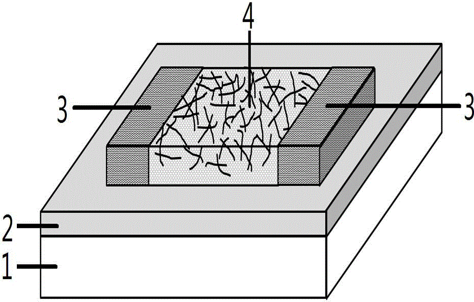
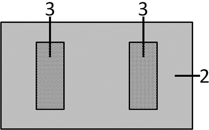
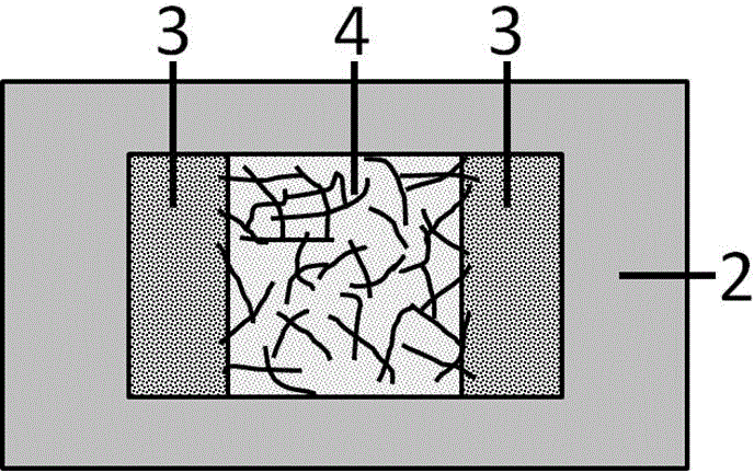
[0018] The present invention is described more specifically in reference examples below with reference to the drawings, and the present invention provides preferred embodiments, but should not be construed as being limited to the embodiments set forth herein. In the drawings, the thicknesses of layers and regions are exaggerated for convenience of illustration, and the shown sizes do not represent actual sizes.

[0019] The referenced figures are schematic illustrations of idealized embodiments of the invention, and the illustrated embodiments of the invention should not be construed as limited to the particular shapes of regions illustrated in the figures but are to include resulting shapes, such as manufacturing-induced deviations. For example, the curves obtained by etching are usually curved or rounded, but in the embodiment of the present invention, they are all represented by rectangles. The representation in the figure is schematic, but this should not be considered as l...


PUM

PropertyMeasurementUnit
thicknessaaaaaaaaaa

Abstract

The invention belongs to the field of microelectronic technologies, and particularly relates to an organic thin-film memory doped with carbon nano tubes. The memory is characterized in that silicon is taken as a substrate gate electrode, the substrate surface oxidizes to form a silicon dioxide insulation layer which acts as a gate dielectric layer, two metal electrodes, which are a source electrode and a drain electrode, are deposited on the insulation layer, a certain distance is reserved between the two electrodes, an organic thin film doped with the carbon nano tubes is deposited between the two electrodes so as to act as a conductive path, and the organic thin film is in contact with the electrodes at the two ends. Storage and erasing of data are realized through applying positive / negative voltage to the substrate (a back gate), and the stored data is read through measuring current of the source electrode and the drain electrode at zero gate voltage. The organic thin-film memory doped with the carbon nano tubes is simple in structure and easy to manufacture and integrate.

Description

technical field [0001] The invention belongs to the technical field of microelectronics, and in particular relates to an organic thin film memory doped with carbon nanotubes. Background technique [0002] Memory plays an important role in the semiconductor world, accounting for 40% of the global semiconductor market, and the replacement speed of memory is very fast. Other semiconductor products other than memory are updated every 2 years, while memory is every 18 years. month generation. As people's requirements for device speed and size continue to increase, the size of integrated circuits continues to decrease and the degree of integration continues to increase. Now it is possible to integrate 2.9 billion transistors in an area the size of a fingernail in a 22nm process. The reduction of the quantum effect will become more and more obvious, resulting in the actual effect of the macro concept, and devices based on the traditional macro concept will not work properly. The ...

Claims


Application Information

Patent Timeline
Patent Type & Authority Applications(China)
IPC IPC(8): H01L51/05H01L51/30H01L51/40
CPCH10K71/12H10K85/221H10K10/00
Inventor 李辉瞿敏妮仇志军张世理刘冉
Owner FUDAN UNIV
Why Eureka
Try Eureka