
Transconductance enhancement mode low voltage transconductance amplifier realized based on complementary metal oxide semiconductor (CMOS) device

A technology of transconductance amplifier and transconductance enhancement, applied in DC-coupled DC amplifiers, differential amplifiers, improved amplifiers to expand bandwidth, etc., can solve the problems of low current utilization efficiency, large power consumption, limited output impedance, etc., and achieve Power saving, low cost, easy integration effect

Inactive Publication Date: 2015-09-23
BEIJING TECHNOLOGY AND BUSINESS UNIVERSITY
View PDF5 Cites 6 Cited by
  • Summary
  • Abstract
  • Description
  • Claims
  • Application Information

AI Technical Summary

Problems solved by technology

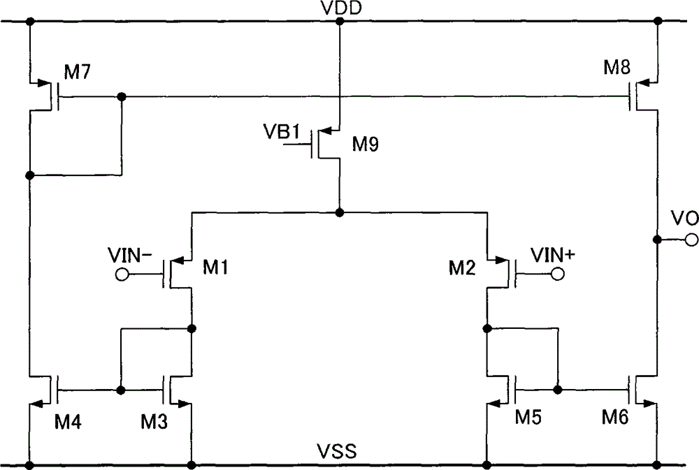
However, this circuit has the disadvantages of insufficient transconductance and limited output impedance:
[0007] 1. The transconductance generated by a single tube is small, which cannot meet the requirements of large bandwidth;
[0008] 2. The output impedance is small, resulting in low amplifier gain, and it is difficult to exceed 40dB under advanced technology;
[0009] 3. Low current utilization efficiency and high power consumption

Method used


Image

  • Transconductance enhancement mode low voltage transconductance amplifier realized based on complementary metal oxide semiconductor (CMOS) device
  • Transconductance enhancement mode low voltage transconductance amplifier realized based on complementary metal oxide semiconductor (CMOS) device
  • Transconductance enhancement mode low voltage transconductance amplifier realized based on complementary metal oxide semiconductor (CMOS) device

Examples


Embodiment Construction

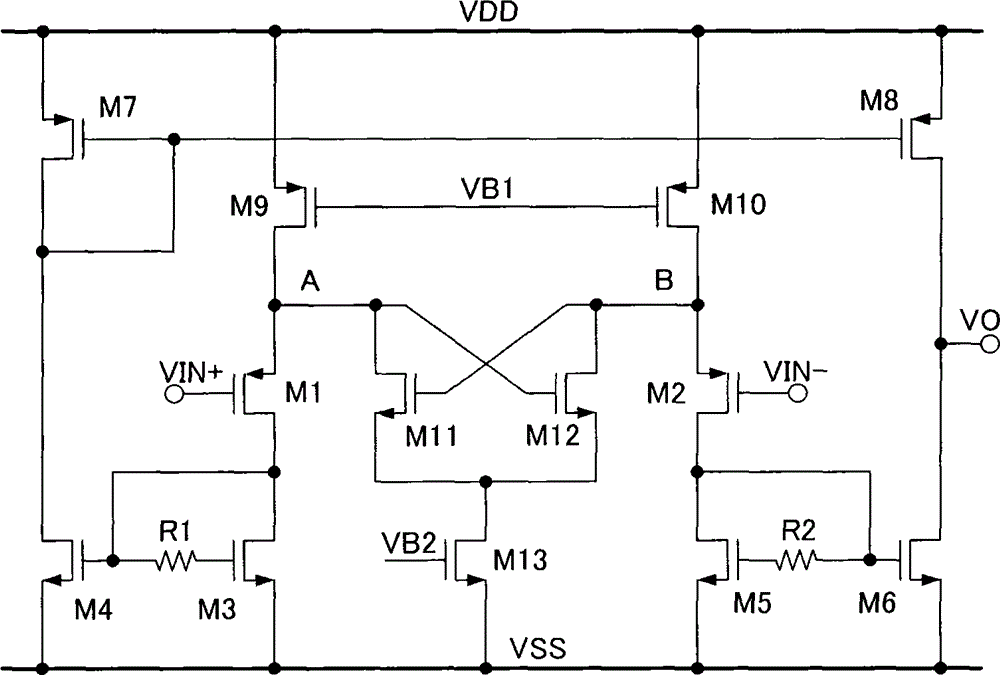
[0024] The transconductance-enhanced low-voltage transconductance amplifier based on CMOS devices proposed by the present invention is implemented in a specific implementation mode using a standard CMOS process. Such as figure 2 As shown, it is characterized in that the transconductance-enhanced low-voltage transconductance amplifier implemented based on CMOS devices includes four major parts: an input differential pair, a positive feedback transconductance enhancement stage, a high-speed current mirror and an output stage.

[0025] The input differential pair is composed of PMOS transistors M1 and M2. The positive feedback transconductance enhancement stage is composed of NMOS transistors M11 and M12, and M13 provides stable current for M11 and M12; the high-speed current mirror is composed of NMOS transistors M3 and M4, M5 and M6, and resistors R1 and R2; The above output stage is composed of M4 and M7, M6 and M8.

[0026] The sources of M1 and M2 are respectively connect...


PUM


Abstract

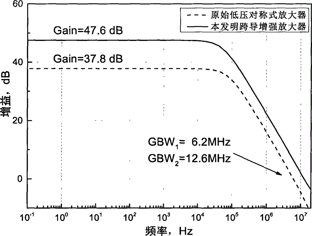
The invention discloses a transconductance enhancement mode low voltage transconductance amplifier realized based on a complementary metal oxide semiconductor (CMOS) device, belonging to the field of design of analog integrated circuits. The amplifier comprises a differential input pair comprising a group of P-channel metal oxide semiconductor (PMOS) pipe and used for converting an input voltage signal into a current signal, a positive feedback diode comprising a group of N-channel metal oxide semiconductor (NMOS) pipe and used for enhancing transconductance through positive feedback, two groups of high-speed current mirrors used for copying an enhanced small signal current, and an output stage comprising NMOS and PMOS pipes and used for providing an output impedance and driving capability. The transconductance enhancement mode low voltage transconductance amplifier has the capability of working at low voltage, can increase the bandwidth by about at least two times compared with an original amplifier, and can save half power consumption, and low frequency gain also has a corresponding enhancement effect. The transconductance enhancement mode low voltage transconductance amplifier realized based on the CMOS device has a good practical prospect, and can be applied to multiple circuit modules, such as signal amplification circuits, AD / DA circuits and so on.

Description

technical field [0001] The invention belongs to the field of analog integrated circuit design, in particular to a transconductance enhanced low-voltage transconductance amplifier based on CMOS devices. Background technique [0002] In recent years, mobile handheld electronic devices have developed rapidly, such as mobile phones, tablet computers, smart wearable devices, etc. People hope that these electronic devices have excellent performance and long-lasting battery life to meet more and more demanding application requirements. In most electronic devices, the integrated circuit chip is a major power-consuming module. Therefore, in chip design, low-power design technology is becoming more and more important, and low-power chips have always been the research focus of academia and industry. [0003] In the field of analog integrated circuit design, the amplifier is a very important circuit module. Most of the analog circuits need to use the amplifier, and the amplifier is als...

Claims


Application Information

Patent Timeline
IPC IPC(8): H03F1/42H03F3/45
Inventor 项辉宇孙超李婷婷杨洋李鹤
Owner BEIJING TECHNOLOGY AND BUSINESS UNIVERSITY
Learn More