TM-structured wafer semi-cut test method

A test method and wafer technology, applied in the direction of semiconductor/solid-state device test/measurement, electrical components, circuits, etc., can solve the problems of reducing the pass rate, increasing the failure rate and mixed batch rate, and reducing the equipment utilization rate. Improve product qualification rate, reduce product scrap rate, and avoid the effect of needle misalignment

Inactive Publication Date: 2015-10-07
NANTONG FUJITSU MICROELECTRONICS
View PDF3 Cites 8 Cited by
  • Summary
  • Abstract
  • Description
  • Claims
  • Application Information

AI Technical Summary

Problems solved by technology

[0006] The biggest problem with the first test method is that when the position or angle of the film is beyond the allowable range of the alignment of the probe station, after the chip is fully cut, the film cannot be re-attached and tested, and the product will be scrapped.
[0008] like figure 1 As shown, after attaching the TM structure wafer to the film, the dicing machine cuts the TM structure wafer completely. When the position or angle of the probe station exceeds the allowable range of alignment of the probe station, an alignment error occurs , the wafer is facing the problem of scrapping; when the probe test is un

Method used


Image

  • TM-structured wafer semi-cut test method
  • TM-structured wafer semi-cut test method
  • TM-structured wafer semi-cut test method

Examples


Example Embodiment

[0022] Embodiments of the present invention will be described below with reference to the drawings. Elements and features described in one drawing or one embodiment of the present invention may be combined with elements and features shown in one or more other drawings or embodiments. It should be noted that representation and description of components and processes that are not related to the present invention and known to those of ordinary skill in the art are omitted from the drawings and descriptions for the purpose of clarity.

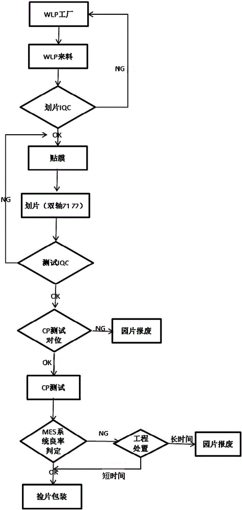
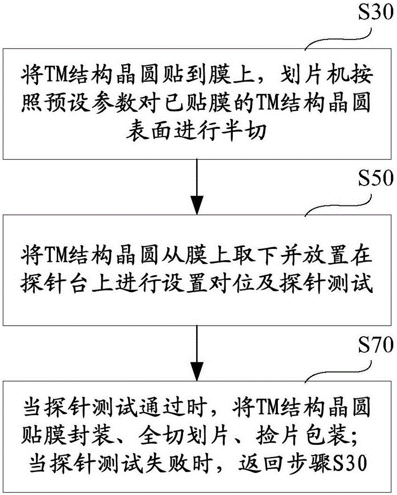
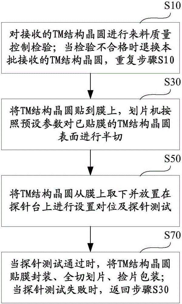
[0023] figure 2 It is a schematic flowchart of an embodiment of the TM structure wafer half-cut testing method of the present invention.

[0024] like figure 2 As shown, in this embodiment, the TM structure wafer testing method of the present invention includes:

[0025] S30: Paste the TM structure wafer on the film, and the dicing machine half-cuts the surface of the film-attached TM structure wafer according to the preset parameters;

[002...


PUM

PropertyMeasurementUnit
Thicknessaaaaaaaaaa

Abstract

The invention provides a TM-structured wafer semi-cut test method. The method comprises the following steps that (S30) a TM-structured wafer is attached to a film; a wafer scriber performs semi-cutting on the surface of the TM-structured wafer with the film attached; (S50) the TM-structured wafer is removed from the film and placed on a probe station for alignment and probe testing; (S70) film attaching, packaging, full-cut scribing and wafer-picking packaging are performed on the TM-structured wafer after the probe tests are passed; and the step S30 is referred to again when the probe tests fail. The risks that the whole wafer cannot be tested due to film attaching deviation can be prevented. The product disability rate can be thus lowered. Conditions of stitching deviation due to a dislocation between bonding pads caused by attaching film contraction and expansion can be prevented. The product yield rate is improved. The wafer picking difficulties during a wafer picking operation can be further prevented. The method provided in the invention has the advantages of simple operations and improved product qualified rate, etc.

Description

technical field [0001] The invention relates to the technical field of semiconductor packaging and testing, in particular to a TM structure wafer half-cut testing method. Background technique [0002] In recent years, under the joint promotion of the cost reduction and the improvement of the front wafer manufacturing process, the semiconductor integrated circuit has achieved the goal of smaller and smaller single chip size of the semiconductor device with the same function, and a new package has been produced. Packaging form WLCSP (Wafer Level Chip Scale Packaging), that is, wafer-level chip-scale packaging, this packaging method is different from the traditional chip packaging method: first cut and then package and test, and at least increase the volume of the original chip by 20% after packaging; The technology is to package and test on the whole wafer first, and then cut into IC particles one by one, so the volume after packaging is equal to the original size of the IC di...

Claims


Application Information

Patent Timeline
IPC IPC(8): H01L21/66
CPCH01L22/34
Inventor 王建镖张健仲伟宏王超黄飞飞
Owner NANTONG FUJITSU MICROELECTRONICS
Why Eureka
Try Eureka