Polarization doping effect-based terahertz diode and process realization method thereof

A polarized doping and terahertz technology, which is applied in the field of microelectronics, can solve problems such as crystal quality influence, low carrier mobility, and device performance, and achieve the goal of improving performance, high mobility, and increasing doping concentration. Effect

Inactive Publication Date: 2015-10-07
HANGZHOU DIANZI UNIV
View PDF4 Cites 4 Cited by
  • Summary
  • Abstract
  • Description
  • Claims
  • Application Information

AI Technical Summary

Problems solved by technology

[0006] Although different measures are adopted, these traditional devices still have the following disadvantages: (1) The activation rate of the traditional impurity doping method is low, and the carrier mobility is low
Since GaN is a wide bandgap semiconductor material, the activation energy of impurities in GaN is very high, resulting in low activation efficiency of doped impurities.
Moreover, the mobility of carriers is low due to the scattering effect of impurity centers
(2) Impurity doping reduces the quality of the crystal a lot and affects the performance of the device
Since the doping of the GaN material system must be carried out while the material is growing, it will inevitably affect the quality of the crystal, thereby affecting the device performance
(3) For devices using the AlGaN thermal electron emission layer, there is a large lattice mismatch between AlGaN and GaN, resulting in a large number of interface defects and affecting device performance

Method used


Image

  • Polarization doping effect-based terahertz diode and process realization method thereof
  • Polarization doping effect-based terahertz diode and process realization method thereof
  • Polarization doping effect-based terahertz diode and process realization method thereof

Examples


Embodiment Construction

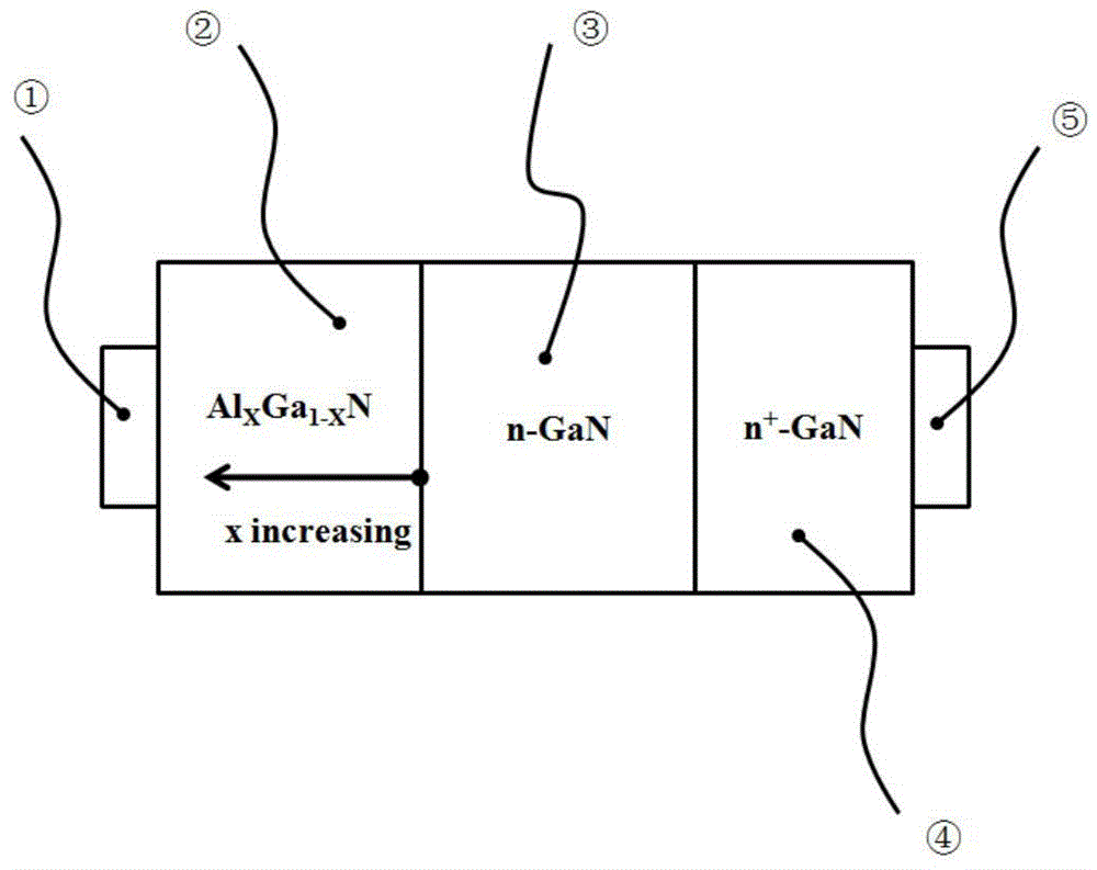
[0032] Such as figure 1 As shown, a terahertz diode based on the polarization doping effect, including the cathode electrode ①, graded Al x Ga 1-x N polarized doped layer ②, active region ③, anode region ④ and anode electrode ⑤;

[0033] The active region is epitaxially grown on the anode region, and the active region is epitaxially grown with graded Al x Ga 1-x N-polarized doped layer; the outside of the anode region is provided with an anode, graded Al x Ga 1-xA cathode is provided outside the N polarized doped layer.

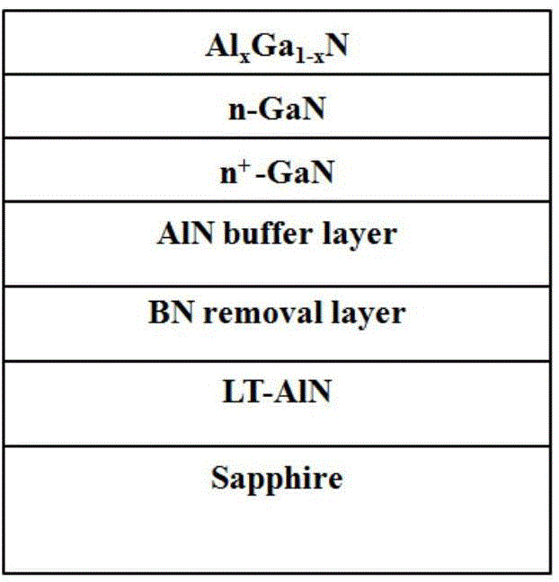
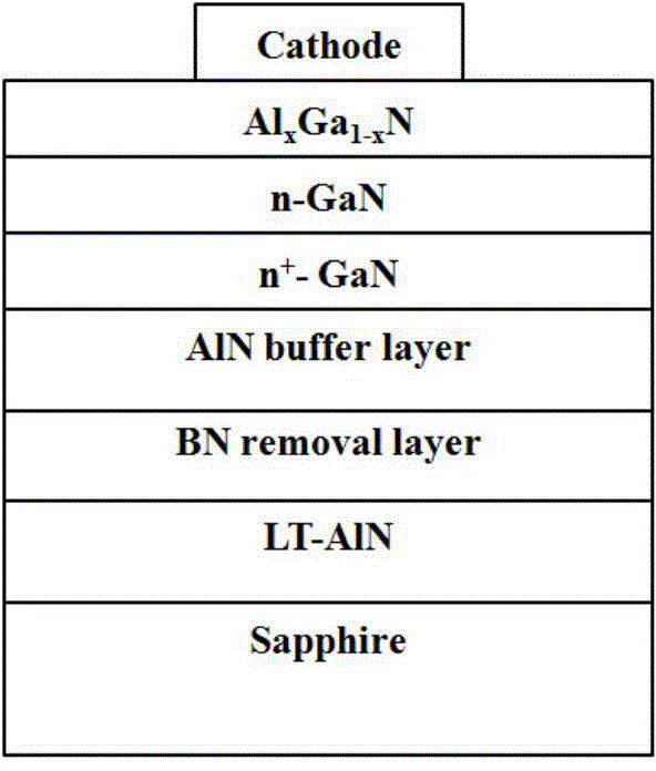
[0034] Such as figure 2 , image 3 , Figure 4 , Figure 5 , Image 6 , Figure 7 , Figure 8 As shown, a process implementation method of a terahertz diode based on the polarization doping effect, the method specifically includes the following steps:

[0035] Step 1: Epitaxial AlGaN / GaN HEMT structure layer on the sapphire substrate by MOCVD or MBE method;

[0036] Step 2: forming a cathode on the front side of the AlGaN / GaN HEMT device;

[0...


PUM

PropertyMeasurementUnit
Thicknessaaaaaaaaaa
Thicknessaaaaaaaaaa
Layer thicknessaaaaaaaaaa

Abstract

The invention discloses a polarization doping effect-based terahertz diode and a process realization method thereof. The device partially comprises a cathode electrode, a gradient AlxGa1-xN polarization doping layer, an active region, an anode region and an anode electrode; the active region is grown on the anode region in an epitaxial manner; the gradient AlxGa1-xN polarization doping layer is grown on the active region in an epitaxial manner; the outer side of the anode region is provided with the anode; and the outer side of the gradient AlxGa1-xN polarization doping layer is provided with the cathode. According to the polarization doping effect-based terahertz diode and the process realization method thereof of the invention, a high-electron density material is adopted, so that electron tunneling can be realized easily, and therefore, excellent ohmic contact can be obtained, and the performance of the device can be improved.

Description

technical field [0001] The invention belongs to the technical field of microelectronics, and in particular relates to a terahertz diode based on a polarization doping effect and a process realization method thereof. Background technique [0002] Terahertz is a wave band between visible light and microwaves. It is a blank field that has not been fully explored by humans so far. Its unique physical properties have very important application prospects in the fields of communication and detection, and have very important scientific research significance. For example , it was considered by the Japanese government as "the top ten science and technology that will change the future". The world's scientific and technological powers have invested manpower and material resources in this field to explore the "treasure" of science and technology. [0003] As the first element of terahertz technology, terahertz emission sources naturally attract the attention of countries all over the wo...

Claims


Application Information

Patent Timeline
IPC IPC(8): H01L29/861H01L29/201H01L29/207H01L29/66
CPCH01L29/8613H01L29/201H01L29/207H01L29/66219
Inventor 董志华程知群刘国华周涛柯华杰
Owner HANGZHOU DIANZI UNIV
Why Eureka
Try Eureka