Substrate having electrical interconnection structure and fabrication method thereof

A technology of electrical connection and electrical contact, applied in the field of substrates with electrical connection structures and their manufacturing methods, capable of solving problems such as poor yield rate of semiconductor packages 1', easy residue of adhesive material 160, poor bonding, etc.

Active Publication Date: 2015-11-04
SILICONWARE PRECISION IND CO LTD
View PDF7 Cites 8 Cited by
  • Summary
  • Abstract
  • Description
  • Claims
  • Application Information

AI Technical Summary

Problems solved by technology

[0016] However, in the above-mentioned conventional manufacturing method of the silicon interposer 1, when the seed layer 13 is etched, part of the copper layer 150 of the metal part 15 will be invalidated, so that an undercut will be formed under the nickel layer 151 and the gold layer 152. (undercut) structure 15', as shown in Figure 1C, so after separating the silicon interposer 1 and the carrier 16, as Figure 1E As shown, the adhesive material 160' is easy to remain under the undercut structure 15', even if the silicon interposer 1 is rinsed with a cleaning liquid (such as water) to remove any residue, there will still be adhesive residue under the undercut structure 15' ( Glue Rsidue)
[0017] In addition, since the adhesive material 160 ′ is adhered to the undercut structure 15 ′, in subsequent processes, when the conductive bump with the solder material 153 is formed, the remaining adhesive material 160 ′ will flow to the conductive bump and the conductive bump. Between the gold layer 152, as Figure 1G As shown, the bonding force between each of the electrical contact pads 101 and the conductive bump is not good, resulting in problems such as poor bonding and poor electrical connection between the semiconductor chip 19 and the silicon interposer 1, thus resulting in the Poor yield of semiconductor package 1'

Method used


Image

  • Substrate having electrical interconnection structure and fabrication method thereof
  • Substrate having electrical interconnection structure and fabrication method thereof
  • Substrate having electrical interconnection structure and fabrication method thereof

Examples


Embodiment Construction

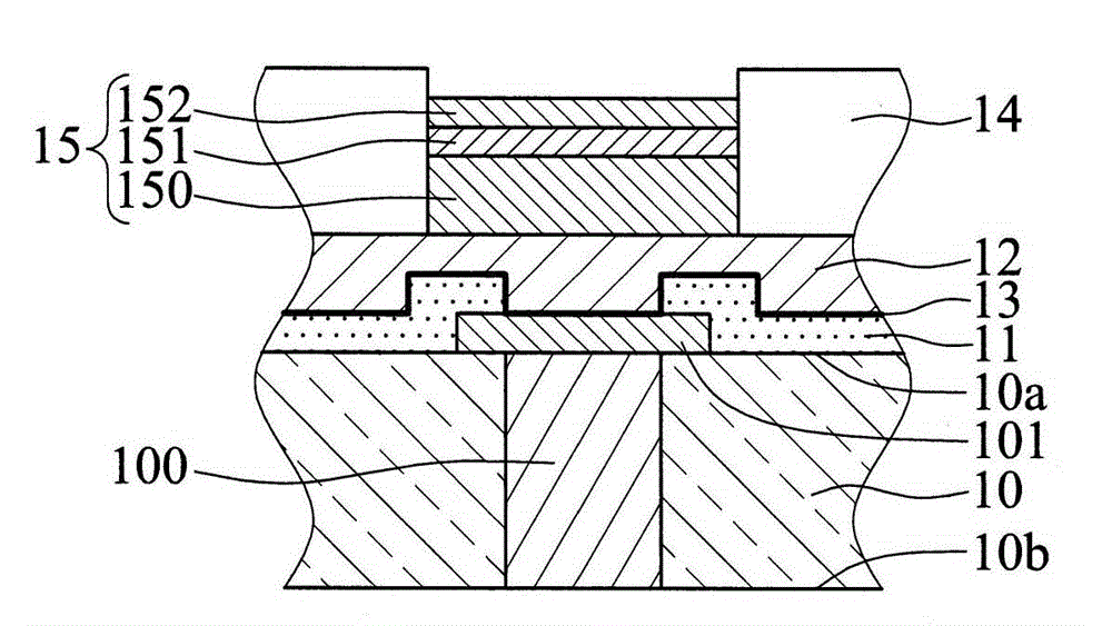
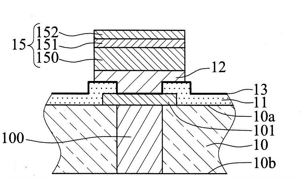
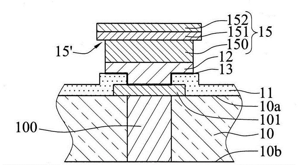
[0111] The embodiments of the present invention are described below through specific specific examples, and those skilled in the art can easily understand other advantages and effects of the present invention from the contents disclosed in this specification.

[0112] It should be noted that the structures, proportions, sizes, etc. shown in the drawings in this specification are only used to cooperate with the contents disclosed in the specification for the understanding and reading of those skilled in the art, and are not used to limit the implementation of the present invention. Restricted conditions, so it does not have technical significance, any modification of the structure, the change of the proportional relationship or the adjustment of the size, without affecting the effect that the present invention can produce and the purpose that can be achieved, should still fall within the present invention. The disclosed technical content must be within the scope of coverage. At...


PUM


Abstract

A method for fabricating a substrate having an electrical interconnection structure is provided, which includes the steps of: providing a substrate body having a plurality of conductive pads and first and second passivation layers sequentially formed on the substrate body and exposing the conductive pads; forming a seed layer on the second passivation layer and the conductive pads; forming a first metal layer on each of the conductive pads, wherein the first metal layer is embedded in the first and second passivation layers without being protruded from the second passivation layer; and forming on the first metal layer a second metal layer protruded from the second passivation layer. As such, when the seed layer on the second passivation layer is removed by etching using an etchant, the etchant will not erode the first metal layer, thereby preventing an undercut structure from being formed underneath the second metal layer.

Description

technical field [0001] The present invention relates to a substrate with an electrical connection structure, in particular to the improved bonding between electrical contact pads and conductive bumps. Background technique [0002] With the vigorous development of the electronic industry, electronic products are gradually moving towards the trend of multi-function and high performance. Technologies currently used in the field of chip packaging, such as Chip Scale Package (CSP), Direct Chip Attached (DCA) or Multi-Chip Module (MCM), etc. Crystal-type packaging modules, or three-dimensional stacking of chips into a three-dimensional integrated circuit (3D IC) chip stacking technology, etc. [0003] The current three-dimensional integrated circuit (3D IC) chip stacking technology, by adding a silicon interposer between the packaging substrate and the semiconductor chip, enables the packaging substrate to be combined with the semiconductor chip with high wiring density electrode...

Claims


Application Information

Patent Timeline
Patent Type & Authority Applications(China)
IPC IPC(8): H01L23/498H01L21/48
CPCC23F1/00H01L21/4857H01L21/486H01L23/147H01L23/49811H01L23/49822H01L23/49827H01L23/49894H01L2224/11H01L2224/16225H01L2224/32225H01L2224/73204H01L2924/15174H01L2924/15311H01L2924/00H05K3/108Y10T29/49165
Inventor 吴柏毅杨侃儒黄晓君庄建隆马光华卢俊宏
Owner SILICONWARE PRECISION IND CO LTD
Why Eureka
Try Eureka