Backside illuminated image chip module structure and fabrication method thereof

A technology of chip module and manufacturing method, which is applied in the direction of radiation control devices, etc., can solve the problems of high packaging cost, difficult to meet, and high cost, and achieve the effect of realizing packaging product cost, simplifying circuit design, and realizing overall cost

Inactive Publication Date: 2015-11-04
NAT CENT FOR ADVANCED PACKAGING
View PDF6 Cites 6 Cited by
  • Summary
  • Abstract
  • Description
  • Claims
  • Application Information

AI Technical Summary

Problems solved by technology

[0003] 1) Existing back-illuminated imaging chips are produced using passive silicon wafers as the carrier board. After entering the packaging neighborhood, TSV through holes need to be made on the passive carrier board to realize the electrical connection of the package, and the cost is relatively high;
[0004] 2) The existing back-illuminated image chip integrates the photosensitive module and image processing module (such as ADC or ISP chip) into one chip, resulting in a small photosensitive area and poor imaging effect under the same chip size; the same photosensitive area and effect Under the conditions, the chip size is large, and it is difficult to meet the needs of consumer electronics for small and thin packages; and the circuit board has high stress and complex structure;
[0005] 3) Currently, TSV packaging on ADC or ISP chips and back-illuminated imaging chips are stacked and packaged at a high cost

Method used


Image

  • Backside illuminated image chip module structure and fabrication method thereof
  • Backside illuminated image chip module structure and fabrication method thereof
  • Backside illuminated image chip module structure and fabrication method thereof

Examples


Embodiment Construction

[0050] The technical solutions of the present invention will be further described below in conjunction with the accompanying drawings and through specific implementation methods.

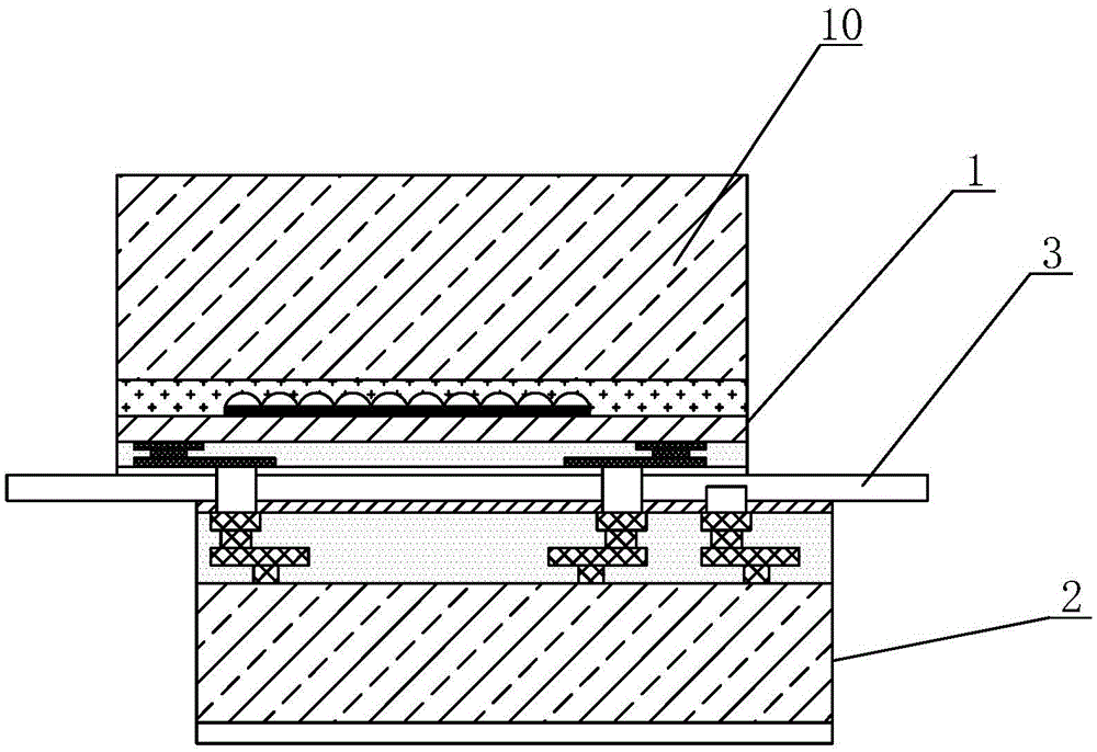
[0051] see Figure 1 to Figure 13As shown, in this embodiment, a back-illuminated image chip module structure includes a BSI chip 1, an ADC chip 2 and a soft board 3, and the ADC chip 2 is arranged under the soft board 3 and is connected to the The flexible board 3 is electrically connected, the BSI chip 1 is arranged on the top of the flexible board 3 and corresponding to the ADC chip 2, and the BSI chip 1 and the ADC chip 2 are directly connected through pads on both.

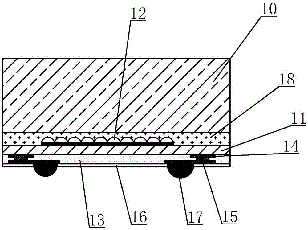
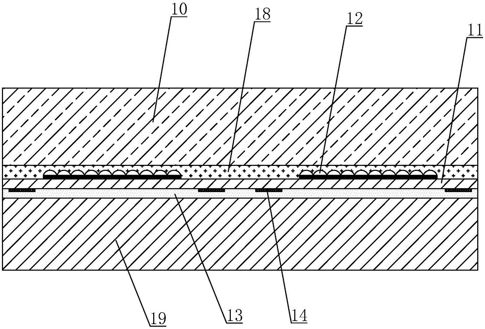
[0052] The BSI chip 1 includes a cover glass 10 and an image chip, the image chip includes a silicon wafer 11, the surface of the silicon wafer 11 is provided with several micro-convex mirrors 12, and its back is provided with a first insulating layer 13 , the first insulating layer 13 is provided with an internal interconnection ...


PUM


Abstract

The invention discloses a backside illuminated image chip module structure and a fabrication method thereof. The fabrication method comprises the following steps of: 1) backside illuminated (BSI) chip packaging, in which a non through silicon vias (TSV) wafer level packaging process is used for BIS chip package; 2) analog-digital converter/image single processor (ISP) chip package; 3) BSI chip and ADC/ISP chip lamination, in which an inversed packaging technique and a surface mounting technology are used for laminating the packaged BIS chip, a soft board and some auxiliary small devices on the ADC/ISP chip or a silicon-base substrate; and 4) lens module installation to finally form an image chip module. By the backside illuminated image chip module structure and the fabrication method thereof, the stress problem between the BSI chip and the soft board is solved, the volume of the whole module is shortened, the circuit design of the soft board is simplified, and the comprehensive cost of the module is reduced.

Description

technical field [0001] The invention belongs to image chip packaging technology, in particular to a back-illuminated image chip module structure and a manufacturing method thereof. Background technique [0002] At present, the packaging structure and process of the back-illuminated image chip (BSI chip) module have the following disadvantages: [0003] 1) Existing back-illuminated imaging chips are produced using passive silicon wafers as the carrier board. After entering the packaging neighborhood, TSV through holes need to be made on the passive carrier board to realize the electrical connection of the package, and the cost is relatively high; [0004] 2) The existing back-illuminated image chip integrates the photosensitive module and image processing module (such as ADC or ISP chip) into one chip, resulting in a small photosensitive area and poor imaging effect under the same chip size; the same photosensitive area and effect Under the conditions, the chip size is large...

Claims


Application Information

Patent Timeline
Patent Type & Authority Applications(China)
IPC IPC(8): H01L27/146
Inventor 张春艳张文奇
Owner NAT CENT FOR ADVANCED PACKAGING
Why Eureka
Try Eureka