LED with P type A1InGaN contact layer, and preparation method thereof

A technology of contact layer and manufacturing method, which is applied in the field of optoelectronics, can solve the problems of shortening the maintenance cycle of MOCVD equipment, unfavorable production stability, etc., and achieve the effects of improving light extraction efficiency, improving surface roughness, and improving quality

Inactive Publication Date: 2015-11-04
SHANDONG INSPUR HUAGUANG OPTOELECTRONICS
View PDF8 Cites 9 Cited by
  • Summary
  • Abstract
  • Description
  • Claims
  • Application Information

AI Technical Summary

Problems solved by technology

However, this patent uses the method of heavy doping of Mg for roughening, which will cause the memory effect of Mg atoms in

Method used


Image

  • LED with P type A1InGaN contact layer, and preparation method thereof

Examples


Embodiment Construction

[0015] Technical scheme of the present invention is as follows:

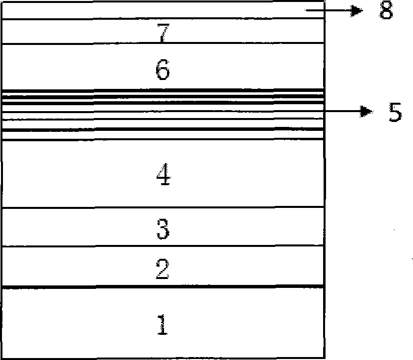
[0016] An LED with a P-type AlInGaN contact layer, its structure includes a substrate, a nucleation layer, a buffer layer, an N-type GaN layer, a multi-quantum well light-emitting layer, and a P-type structure from bottom to top; wherein,

[0017] The nucleation layer is one of a gallium nitride layer, an aluminum nitride layer or an aluminum gallium nitride layer;

[0018] The buffer layer is a non-doped GaN layer;

[0019] The multi-quantum well light-emitting layer is composed of InGaN potential well layers and GaN barrier layers alternately stacked periodically;

[0020] The composition of the P-type structure is a P-type AlGaN layer, a P-type GaN layer and a P-type AlInGaN contact layer in sequence.

[0021] Preferably, according to the present invention, the multi-quantum well light-emitting layer has 5-20 periods.

[0022] The above-mentioned preparation method of an LED with a P-type AlInGaN contact l...


PUM

PropertyMeasurementUnit
Thicknessaaaaaaaaaa
Thicknessaaaaaaaaaa
Thicknessaaaaaaaaaa

Abstract

The invention relates to an LED with a P type A1InGaN contact layer, and a preparation method thereof. The structure successively comprises a substrate, a nucleation layer, a buffer layer, an N type GaN layer, a multi-quantum well luminescent layer, and a P type structure from bottom to top; wherein the P type structure is successively composed of a P type A1GaN layer, a P type GaN layer and a P type A1InGaN contact layer. The In doping amount in the P type A1InGaN layer of an LED chip changes regularly, thereby changing the energy band distribution of the P type A1InGaN layer, weakening the blocking effect of the valance band of the P type A1InGaN layer in hole injection, and meanwhile not weakening the blocking effect to other electrons. The structure can improve surface coarsening to a certain degree; through the structure, the ohmic contact of the LED chip can be reduced by about 10%.

Description

technical field [0001] The invention relates to an LED with a P-type AlInGaN contact layer and a preparation method thereof, belonging to the field of optoelectronic technology. Background technique [0002] In the early 1990s, the third-generation wide-bandgap semiconductor materials represented by nitrides made a historic breakthrough. Researchers successfully prepared blue-green and ultraviolet LEDs on gallium nitride materials, making LED lighting become possible. In 1971, the first gallium nitride LED die came out. In 1994, gallium nitride HEMTs appeared blue light GaN-based diodes with high electron mobility, and gallium nitride semiconductor materials developed very rapidly. [0003] Semiconductor light-emitting diodes have the advantages of small size, ruggedness, strong controllability of light-emitting bands, high luminous efficiency, low heat loss, low light decay, energy saving, and environmental protection. Communication and other fields have a wide range of a...

Claims


Application Information

Patent Timeline
IPC IPC(8): H01L33/14H01L33/00
Inventor 逯瑶王成新曲爽
Owner SHANDONG INSPUR HUAGUANG OPTOELECTRONICS
Why Eureka
Try Eureka