LED having N type AlInGaN contact layer and preparation method

A contact layer, N-type technology, applied in the field of optoelectronics, can solve problems such as unfavorable production stability, shorten the maintenance cycle of MOCVD equipment, etc., and achieve the effects of improving the quality of P-type GaN films, improving external quantum efficiency, and increasing hole concentration.

Inactive Publication Date: 2015-12-16
SHANDONG INSPUR HUAGUANG OPTOELECTRONICS
View PDF8 Cites 4 Cited by
  • Summary
  • Abstract
  • Description
  • Claims
  • Application Information

AI Technical Summary

Problems solved by technology

However, this method uses the method of heavily doping Mg for roughening, which will cause the memory effect of Mg atoms in the reaction chamber, shorten the maintenance cycle of MOCVD equipment, and is not conducive to the stability of production.

Method used


Image

  • LED having N type AlInGaN contact layer and preparation method

Examples


Embodiment 1

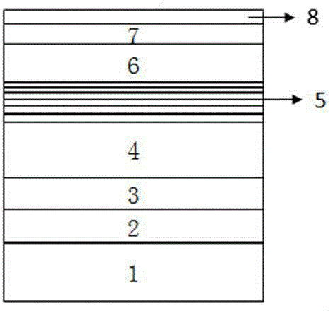
[0036] LED with N-type AlInGaN contact layer of the present invention such as figure 1 As shown, it includes substrate 1, nucleation layer 2, buffer layer 3, N-type GaN layer 4, multi-quantum well light-emitting layer 5 and P-type structure from bottom to top, and the P-type structure is P-type AlGaN layer 6, P-type GaN layer 7 and N-type AlInGaN contact layer 8 .

[0037] In this embodiment, the substrate 1 is a silicon carbide substrate. The nucleation layer 2 is an aluminum nitride layer with a thickness of 30 nm. The buffer layer 3 is a non-doped GaN layer with a thickness of 2 μm. The thickness of the N-type GaN layer 4 is 2 μm. The multi-quantum well light-emitting layer 5 is composed of 15 cycles of InGaN potential well layers and GaN barrier layers alternately superimposed, with a total thickness of 225nm. In a single cycle, the thickness of the InGaN potential well layer is 3nm, and the thickness of the GaN barrier layer is 12nm. The Mg doping concentration in the...

Embodiment 2

[0049] In this embodiment, the substrate 1 is a sapphire substrate. The nucleation layer 2 is an AlGaN layer with a thickness of 120nm. The buffer layer 3 is a non-doped GaN layer with a thickness of 1.8 μm. The thickness of the N-type GaN layer 4 is 2.5 μm. The multi-quantum well light-emitting layer 5 is composed of 18 periods of InGaN potential well layers and GaN barrier layers alternately superimposed, with a total thickness of 270nm. In a single period, the thickness of the InGaN potential well layer is 2nm, and the thickness of the GaN barrier layer is 14nm. . The Mg doping concentration in the P-type AlGaN layer 6 is 9.8×10 18 / cm -3 . The Mg doping concentration in the p-type GaN layer 7 is 8×10 19 / cm -3 . The thickness of the N-type AlInGaN contact layer 8 is 80 nm.

[0050] The preparation process of the above-mentioned LED having an N-type AlInGaN contact layer specifically includes the following steps:

[0051] (1) Put the sapphire substrate in the reac...

Embodiment 3

[0061] In this embodiment, the substrate 1 is a sapphire substrate. The nucleation layer 2 is a gallium nitride layer with a thickness of 600nm. The buffer layer 3 is a non-doped GaN layer with a thickness of 1.5 μm. The thickness of the N-type GaN layer 4 is 1.5 μm. The multi-quantum well light-emitting layer 5 is composed of 12 periods of InGaN potential well layers and GaN barrier layers alternately superimposed, with a total thickness of 210nm. In a single period, the thickness of the InGaN potential well layer is 3.5nm, and the thickness of the GaN barrier layer is 14nm. The Mg doping concentration in the P-type AlGaN layer 6 is 1.2×10 18 / cm -3 . The Mg doping concentration in the p-type GaN layer 7 is 5×10 19 / cm -3 . The thickness of the N-type AlInGaN contact layer 8 is 2 nm.

[0062] The preparation process of the above-mentioned LED having an N-type AlInGaN contact layer specifically includes the following steps:

[0063] (1) Put the sapphire substrate in ...


PUM


Abstract

An LED having an N type AlInGaN contact layer and a preparation method. The structure comprises a substrate, a nucleating layer, a buffer layer, an N type GaN layer, a multi-quantum-well luminous layer and a P type structure in sequence from bottom to top, and the P type structure includes a P type AlGaN layer, a P type GaN layer and an N type AlInGaN contact layer in sequence. The nucleating layer, the buffer layer, the N type GaN layer, the multi-quantum-well luminous layer, the P type AlGaN layer, the P type GaN layer and the N type AlInGaN layer are grown on the substrate in sequence, through regular changes of the doping amount of In in the N type AlInGaN layer arranged in an LED chip, energy band distribution of the N type AlInGaN layer is changed, a blocking effect of a valence band of the N type AlInGaN layer on hole injection is weakened while a blocking effect on electrons is not weakened, surface roughness can be improved to some extent, and ohmic contact of the LED chip can be reduced by about 10%.

Description

technical field [0001] The invention relates to an LED (light-emitting diode) with an N-type AlInGaN contact layer and a preparation method thereof, belonging to the field of optoelectronic technology. Background technique [0002] In the early 1990s, the third-generation wide-bandgap semiconductor materials represented by nitrides made a historic breakthrough. Researchers successfully prepared blue-green and ultraviolet LEDs on gallium nitride materials, making LED lighting become possible. In 1971, the first gallium nitride LED die came out. In 1994, gallium nitride HEMTs appeared blue light GaN-based diodes with high electron mobility, and gallium nitride semiconductor materials developed very rapidly. [0003] Semiconductor light-emitting diodes have the advantages of small size, ruggedness, strong controllability of light-emitting bands, high luminous efficiency, low heat loss, low light decay, energy saving, and environmental protection. Communication and other field...

Claims


Application Information

Patent Timeline
Patent Type & Authority Applications(China)
IPC IPC(8): H01L33/40H01L33/02
CPCH01L33/40H01L33/0066H01L33/0075H01L33/025
Inventor 逯瑶曲爽王成新徐现刚
Owner SHANDONG INSPUR HUAGUANG OPTOELECTRONICS
Why Eureka
Try Eureka