Method for Improving Contact Hole Morphology of Semiconductor Devices

A contact hole and semiconductor technology, which is applied in semiconductor/solid-state device manufacturing, electrical components, circuits, etc., can solve problems such as adverse effects on product reliability, achieve low cost and improve reliability

Active Publication Date: 2017-10-24
SHANGHAI HUAHONG GRACE SEMICON MFG CORP
View PDF5 Cites 0 Cited by
  • Summary
  • Abstract
  • Description
  • Claims
  • Application Information

AI Technical Summary

Problems solved by technology

[0012] like figure 2 Shown is the electron micrograph of the contact hole of the IGBT formed by the existing method; it can be seen that a peak is formed in the top area of ​​the contact hole, that is, the area shown in the dotted box 101, and the peak is due to the wet etching process of the top area. Lateral etching will occur, causing a peak to form at the connection position between the top area and the bottom area formed by wet etching and dry etching. The existence of this peak will generate a peak electric field, which will adversely affect the reliability of the product

Method used


Image

  • Method for Improving Contact Hole Morphology of Semiconductor Devices
  • Method for Improving Contact Hole Morphology of Semiconductor Devices
  • Method for Improving Contact Hole Morphology of Semiconductor Devices

Examples


Embodiment Construction

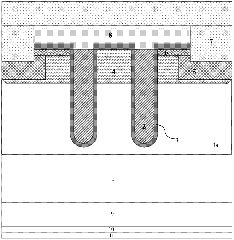
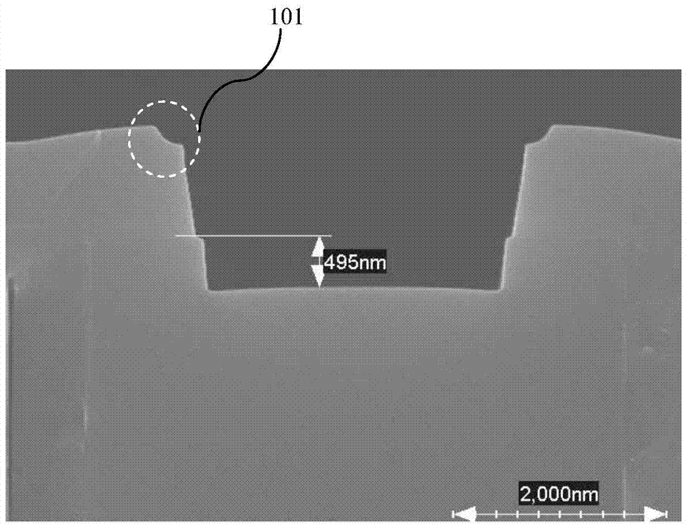
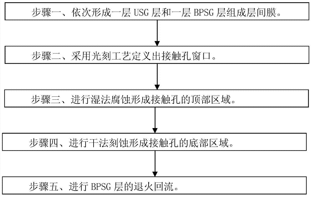
[0033] Such as image 3 Shown is the flow chart of the method of the embodiment of the present invention; in the embodiment of the present invention, the semiconductor device is as figure 1 The IGBT device shown is illustrated as an example for forming figure 1 shown in the contact hole 7. The method for improving the morphology of a contact hole of a semiconductor device in an embodiment of the present invention includes the following steps:

[0034] Step 1, on the semiconductor substrate where contact holes need to be formed, namely figure 1 A USG layer and a BPSG layer are sequentially formed on the surface of the N-type substrate 1 shown, and an interlayer film 8 is formed by superimposing the USG layer and the BPSG layer, which is performed before annealing and reflowing the BPSG layer. Follow steps 2 to 4.

[0035] In the embodiment of the present invention, the thickness of the USG layer is 2000 angstroms, and the thickness of the BPSG layer is 9000 angstroms.

[0...


PUM


Abstract

The present invention discloses a method for improving appearance of a contact hole of a semiconductor device, comprising: a first step of successively forming one layer of USG layer and one layer of BPSG layer to form an interlayer film; a second step of defining a contact hole window through photolithographic process; a third step of performing wet etching to form a top area of a contact hole; a fourth step of performing dry etching to form a bottom area of the contact hole; and a fifth step of performing annealing backflow of the BPSG layer. The method of the present invention can make the appearance of the contact hole smooth, can eliminate a peak structure, and can improve reliability of the device.

Description

technical field [0001] The invention relates to a method for manufacturing a semiconductor integrated circuit, in particular to a method for improving the morphology of a contact hole of a semiconductor device. Background technique [0002] Insulated Gate Bipolar Transistor (IGBT) is a composite fully-controlled voltage-driven power semiconductor device composed of a bipolar transistor (BJT) and an insulated gate field effect transistor (MOSFET). A giant transistor (Giant Transistor, GTR) that can work at high voltage and high current is also a power transistor; IGTB has the advantages of high input impedance of MOSFET and low conduction voltage drop of GTR. It is very suitable for the conversion system with a DC voltage of 600V and above, such as AC motors, frequency converters, switching power supplies, lighting circuits, traction drives and other fields. [0003] For the IGBT process, forming a good contact hole morphology can greatly improve the reliability of the devic...

Claims


Application Information

Patent Timeline
Patent Type & Authority Patents(China)
IPC IPC(8): H01L21/768
CPCH01L21/7684
Inventor 马彪
Owner SHANGHAI HUAHONG GRACE SEMICON MFG CORP
Why Eureka
Try Eureka