Light-emitting diode epitaxial structure containing AlGaN conducting layer, and manufacturing method thereof

A technology of light-emitting diodes and epitaxial structures, applied in circuits, electrical components, semiconductor devices, etc., can solve problems such as low efficiency and low internal quantum efficiency, and achieve the effects of improving efficiency, improving internal quantum efficiency, and suppressing electron leakage

Inactive Publication Date: 2015-11-11
SOUTH CHINA UNIV OF TECH
View PDF6 Cites 8 Cited by
  • Summary
  • Abstract
  • Description
  • Claims
  • Application Information

AI Technical Summary

Problems solved by technology

[0008] Aiming at the problem of low internal quantum efficiency caused by the overflow of electrons from the multi-quantum well active area and the low efficiency of hole injection into the multi-quantum well active area in the existi...

Method used


Image

  • Light-emitting diode epitaxial structure containing AlGaN conducting layer, and manufacturing method thereof
  • Light-emitting diode epitaxial structure containing AlGaN conducting layer, and manufacturing method thereof
  • Light-emitting diode epitaxial structure containing AlGaN conducting layer, and manufacturing method thereof

Examples


Embodiment Construction

[0031] The present invention will be further described below in conjunction with the accompanying drawings and examples, but not limited thereto.

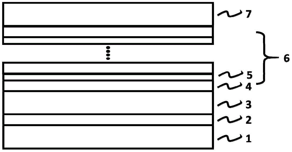
[0032] Such as figure 1 As shown, the light emitting diode epitaxy includes sapphire substrate 1 , GaN buffer layer 2 , N-type GaN conductive layer 3 , multi-quantum well active region 6 and P-type AlnGaN conductive layer 7 from bottom to top.

[0033] The steps of the method for preparing a light emitting diode epitaxial structure with an AlGaN conductive layer are as follows:

[0034] (1). Put the sapphire substrate into the metal-organic chemical vapor phase chemical deposition equipment, pass in hydrogen, raise the temperature of the reaction chamber to 1300 degrees Celsius, and perform high-temperature cleaning on the substrate.

[0035] (2). Reduce the temperature of the reaction chamber to 1100 degrees, feed ammonia, hydrogen and trimethylgallium, and grow a 3um unintentionally doped GaN buffer layer on the substrate descri...


PUM

PropertyMeasurementUnit
Thicknessaaaaaaaaaa

Abstract

The invention discloses a light-emitting diode epitaxial structure containing a AlGaN conducting layer, and a manufacturing method thereof. The epitaxial structure is composed of a substrate, a GaN buffer layer, an N type GaN conductive layer, a multi-quantum-well active region and a P type AlGaN conducting layer. The P type conducting layer is made of analuminum-contained AlGaN material and Al components in the AlGaN layer are gradually increased linearly along the growth direction. Accoridng to the invention, with the P type AlGaN conducting layer, barriers for blocking injection of holes into the multi-quantum-well active region at the P type AlGaN electronic blocking layer and the P type GaN conducting layer can be avoided. Because the Al components in the P type AlGaN conducting layer are gradually increased along the growth direction, the polarized charge density, the polarized electric field intensity of the quantum well, and the band bending can be reduced, the electron overflowing blocking effect of the P type AlGaN conducting laywer can be enhanced, and the hole injection blocking can be weakened.

Description

technical field [0001] The invention relates to the technical field of light-emitting diodes, in particular to an epitaxial structure of a light-emitting diode with an aluminum-containing conductive layer having a graded aluminum composition and a preparation method thereof. Background technique [0002] A light-emitting diode (referred to as "LED") is a semiconductor solid-state light-emitting device. It uses the conduction band electrons and valence band holes inside the semiconductor material to undergo radiative recombination, and releases energy in the form of photons to directly emit light. By designing different bandgap widths of semiconductor materials, light-emitting diodes can emit light in different bands from infrared to ultraviolet. [0003] Nitride light-emitting diodes have been widely developed around the world due to their advantages of high efficiency, energy saving, long life and small size. Ultraviolet light-emitting diodes with a light emission waveleng...

Claims


Application Information

Patent Timeline
IPC IPC(8): H01L33/14H01L33/06H01L33/00
CPCH01L33/007H01L33/06H01L33/14
Inventor 徐明升周泉斌王洪
Owner SOUTH CHINA UNIV OF TECH
Why Eureka
Try Eureka