Unsealing method for flip-chip packaging device

A technology for packaging devices and flip-chips, which is applied in the field of semiconductor integrated circuit testing, can solve the problems of unsealing of sealed devices, failure of unsealing, insufficient grinding, etc., and achieves difficult to control etching accuracy, poor adaptability, and guarantees the quality of unsealing. Effect

Inactive Publication Date: 2015-11-25
METROLOGY & MEASUREMENT CENT OF CHINA ACADEMY OF ENG PHYSICS
View PDF8 Cites 17 Cited by
  • Summary
  • Abstract
  • Description
  • Claims
  • Application Information

AI Technical Summary

Problems solved by technology

[0006] 1. The existing methods are only for plastic-encapsulated devices, and cannot solve the problem of unsealing sealed devices
[0007] 2. For multi-chip devices (more than two chips are assembled in the same tooling), the chip solder joints are easily treated as substrate through holes, resulting in excessive grinding and failure of unsealing
[0008] 3. The existing method relies heavily on the experience of the operator, and the problem of insufficient or excessive grinding is prone to occur when grinding the sample, resulting in the failure of unsealing

Method used


Image

  • Unsealing method for flip-chip packaging device
  • Unsealing method for flip-chip packaging device

Examples


Embodiment 1

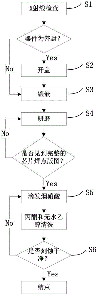
[0033] like figure 1 As shown, the present invention provides a method for unsealing a flip-chip packaged device, comprising the steps of:

[0034] S1), inspect the device in the Y-axis and X-axis, and obtain clear X-ray photos of the device in two directions. The Y-axis inspection is to obtain the chip solder joint layout photos of the device to prepare for grinding; the X-axis inspection is mainly to determine the structure of the device in the vertical direction and the thickness of the substrate material to ensure that the quality of the grinding process is controllable.

[0035] S2), open the sealed device (this step is only for sealed devices)

[0036] If the device is a sealed type, the sealing cover of the device must be opened first. The sealing cover is mostly bonded to the substrate by metal and ceramic. The metal sealing cap can be opened with a sharp knife; the ceramic sealing cap can be opened with a pliers-type capping machine. The purpose of opening the cov...

Embodiment 2

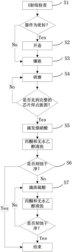
[0048] like figure 2 As shown, the present invention provides a method for unsealing a flip-chip packaged device, comprising the following steps:

[0049] S1), X-ray inspection is performed on the device, and X-ray photos of the device are obtained; preferably, X-ray inspections are performed on the device in the X-axis and Y-axis respectively, and X-ray photos in two directions of the device are obtained.

[0050] S3), perform device embedding; preferably, in this step, place the device substrate horizontally in the embedding equipment facing downward. In order to prevent the device from moving and turning over during the mounting process, a small amount of double-sided adhesive tape was pasted on the sample stage of the mounting equipment to fix the device. When potting powder or mounting liquid, it should be added slowly to prevent the device from being washed away. Since the hot mounting process will generate high temperature and high pressure, in order to prevent chip ...


PUM


Abstract

A related unsealing method for a flip-chip packaging device comprises the following steps: S100) performing X-ray detection on the device, so as to obtain a device X-ray photograph; S200) performing device inlaying; S300) performing grinding on the inlayed device by taking the X-ray photograph as a reference; S400) performing acid dropping and cleaning on the ground device; S500) performing microscope detection, returning to the step S400) is the chip surface residue is detected, and stopping until the chip surface etching is clean. The beneficial effects comprise that the method is applicable to all flip-chip packaging devices at present, and comprises sealing, ceramic packaging and plastic packaging; through X-ray detection, the chip welding spot layout is determined, the grinding ending point can be precisely determined, and insufficient grinding and excessive grinding are both avoided; and through the process of manually dropping an acid and performing microscope detection and dropping the acid again, the etching degree is strictly controlled, the unsealing quality is guaranteed, and the welding spots and boding spots of a chip are prevented from being automatically excessively corroded.

Description

technical field [0001] The invention belongs to the technical field of detection of semiconductor integrated circuits, and in particular relates to a method for unsealing a flip-chip packaging device. Background technique [0002] Flip-chip packaging is an advanced form of semiconductor integrated circuit packaging. Its specific operation method is to create solder joints on the chip, and then flip the chip and solder it to the substrate. Since this packaging form can greatly increase the input and output (I / O) port density of the device and reduce the size and weight of the device, and simplifies the process to reduce the cost and reduce the parasitic effect of the package, it is used in the integrated circuit Packaging is used more and more widely. [0003] However, the structure of chip undercut brings difficulties to destructive physical analysis (DPA) detection and failure analysis (FA) of electronic components. Because these two types of tests need to unpack the devi...

Claims


Application Information

Patent Timeline
Patent Type & Authority Applications(China)
IPC IPC(8): G01N1/28G01N1/32
Inventor 何志刚
Owner METROLOGY & MEASUREMENT CENT OF CHINA ACADEMY OF ENG PHYSICS
Why Eureka
Try Eureka