Display device, pixel circuit thereof and driving method thereof

A pixel circuit and current technology, which is applied in the field of display devices, can solve problems such as uneven light emission of pixels and low aperture ratio of pixel circuits, and achieve the effects of reducing voltage distortion, increasing uniformity, and uniform brightness

Active Publication Date: 2015-11-25
PEKING UNIV SHENZHEN GRADUATE SCHOOL
View PDF5 Cites 14 Cited by
  • Summary
  • Abstract
  • Description
  • Claims
  • Application Information

AI Technical Summary

Problems solved by technology

However, some pixel circuits use a complex circuit structure and more data control lines, so that the aperture ratio of the pixel circuit is relatively low.
In order to obtain a higher resolution display, some pixel circuits use the method of reducing the area of ​​the storage capacitor, but this will lead to uneven light emission of the pixels

Method used


Image

  • Display device, pixel circuit thereof and driving method thereof
  • Display device, pixel circuit thereof and driving method thereof
  • Display device, pixel circuit thereof and driving method thereof

Examples


Embodiment 1

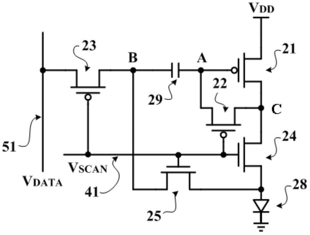
[0050] like figure 2 Shown is a structural diagram of the pixel circuit of the first embodiment, including a first transistor 21, a second transistor 22, a third transistor 23, a fourth transistor 24, a fifth transistor 25, a light-emitting device 28, a capacitor 29, and a first scan control. Signal line 41 and data signal line 51 .

[0051] The first transistor 21, the second transistor 22 and the third transistor 23 are P-type transistors; the fourth transistor 24 and the fifth transistor 25 are N-type transistors; the first transistor 21, the fourth transistor 24 and the light-emitting device 28 are connected in series with the power supply voltage line and ground level.

[0052] The control electrode of the first transistor 21 is coupled to the first current conducting electrode of the capacitor 29 , the first current conducting electrode of the first transistor 21 is coupled to the second current conducting electrode of the second transistor 22 , and the first current c...

Embodiment 2

[0073] like Figure 5 Shown is the structure diagram of the pixel circuit according to the second embodiment of the present invention, including a first transistor 21, a second transistor 22, a third transistor 23, a fourth transistor 24, a fifth transistor 25, a light-emitting device 28, a capacitor 29, a first transistor The scan control signal line 41 , the second scan control signal line 42 and the data signal line 51 . The main difference between the device selection and the first embodiment is that the fourth transistor 24 and the fifth transistor 25 are P-type transistors. The circuit adopts the circuit structure of all P-type tubes, which can reduce the process complexity in the manufacturing process. The devices whose connection relationship has not changed in the circuit will not be repeated here. The difference in the circuit connection is that the control electrode of the fourth transistor 24 is coupled to the second scan control signal line 42, and the first curr...

Embodiment 3

[0088] like Figure 8 As shown, the pixel circuit in this embodiment includes a first transistor 21, a second transistor 22, a third transistor 23, a fourth transistor 24, a fifth transistor 25, a light-emitting device 28, a capacitor 29, and a first scan control signal line 41 and data signal line 51 .

[0089]The first transistor 21, the fourth transistor 24 and the fifth transistor 25 are P-type transistors, the second transistor 22 and the third transistor 23 are N-type transistors; the first transistor 21, the fourth transistor 24 and the light-emitting device 28 are connected in series to the first between the supply voltage line and the ground level.

[0090] The control electrode of the first transistor 21 is coupled to the first current conducting electrode of the capacitor 29 , the first current conducting electrode of the first transistor 21 is coupled to the first current conducting electrode of the second transistor 22 , and the first current conducting electrode...


PUM


Abstract

The invention discloses a display device, a pixel circuit thereof and a driving method thereof. The pixel circuit provided by the invention comprises a first transistor, a second transistor, a third transistor, a fourth transistor, a fifth transistor and a capacitor element. The first transistor is used for providing a driving current to a light emitting device. The second transistor, the third transistor, the fourth transistor and the fifth transistor serve as switch tubes and are used for responding to scanning signals. The capacitor element is used for storing voltage information and coupling the voltage information to a control electrode of the first transistor so as to enable the first transistor to generate a drain current for driving the light emitting device. The pixel circuit is capable of preventing the problem of the switch tubes that light illumination brightness is uneven due to charge leakage under a switched-off state and is capable of compensating the change or uneven phenomenon of a first threshold voltage for driving the transistors; in addition, under the condition that the storage capacitance is very small, the compensation voltage in one frame is maintained by a negative feedback structure, the distortion of the voltage is reduced, and the uniform degree of brightness is improved. By adopting the pixel circuit provided by the invention, a display high in resolution can be manufactured.

Description

technical field [0001] The present invention relates to the field of display devices, in particular to a display device, a pixel circuit and a driving method thereof. Background technique [0002] OLED (Organic Light-Emitting Diode, Organic Light Emitting Diode) display has been widely studied in recent years due to its advantages of active light emission, high brightness, high luminous efficiency, wide viewing angle, low power consumption, and low manufacturing cost. display device. OLED display can be divided into PMOLED (Passive Matrix OLED, passive matrix OLED) and AMOLED (Active Matrix OLED: active matrix OLED) according to the pixel driving method. Although PMOLED has low manufacturing cost, it has crosstalk and requires large driving current, so it has the disadvantages of short service life and high power consumption, and cannot meet the display requirements of large area and high resolution. In contrast, AMOLED avoids issues such as duty cycle and crosstalk, and r...

Claims


Application Information

Patent Timeline
Patent Type & Authority Applications(China)
IPC IPC(8): G09G3/32
Inventor 张盛东王翠翠冷传利鲁文高陈中建张雅聪
Owner PEKING UNIV SHENZHEN GRADUATE SCHOOL
Why Eureka
Try Eureka