
Manufacturing method of silicon wafer and silicon wafer

A manufacturing method and technology for silicon wafers, which are applied in semiconductor/solid-state device manufacturing, electrical components, circuits, etc., and can solve the problems of reduced haze level and insufficient haze level.

Active Publication Date: 2018-11-23
SUMCO CORP
View PDF5 Cites 0 Cited by
  • Summary
  • Abstract
  • Description
  • Claims
  • Application Information

AI Technical Summary

Problems solved by technology

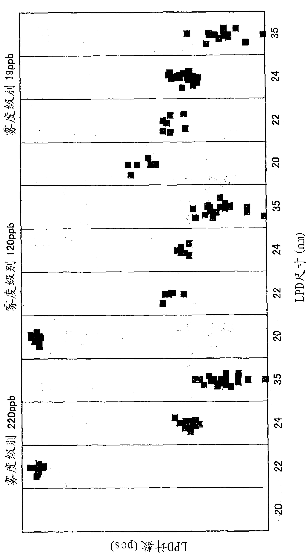
[0005] However, the haze level described in the above-mentioned Patent Document 1 is insufficient in view of the need to measure particles of finer particle diameters as silicon wafers are required to have high cleanliness, and further reduction of the haze level is required.

Method used


Image

  • Manufacturing method of silicon wafer and silicon wafer
  • Manufacturing method of silicon wafer and silicon wafer
  • Manufacturing method of silicon wafer and silicon wafer

Examples


Embodiment approach

[0079] In addition, the present invention is not limited to the above-described embodiments, and various improvements, design changes, and the like can be made without departing from the gist of the present invention.

[0080] In the above-mentioned embodiment, the case where at least hydrogen fluoride cleaning is performed in the cleaning step has been described. However, in addition to the above-mentioned hydrogen fluoride cleaning, it is also possible to perform brush cleaning in which the brush is brought into sliding contact with the front surface of the wafer to remove dirt on the front surface of the wafer. The element that becomes the hydrogen termination on the front side of the wafer. By using the scrub together, the hydrogen termination rate on the front side of the wafer can be increased more efficiently. In addition, it is preferable that this scrubbing is performed before hydrogen fluoride cleaning.

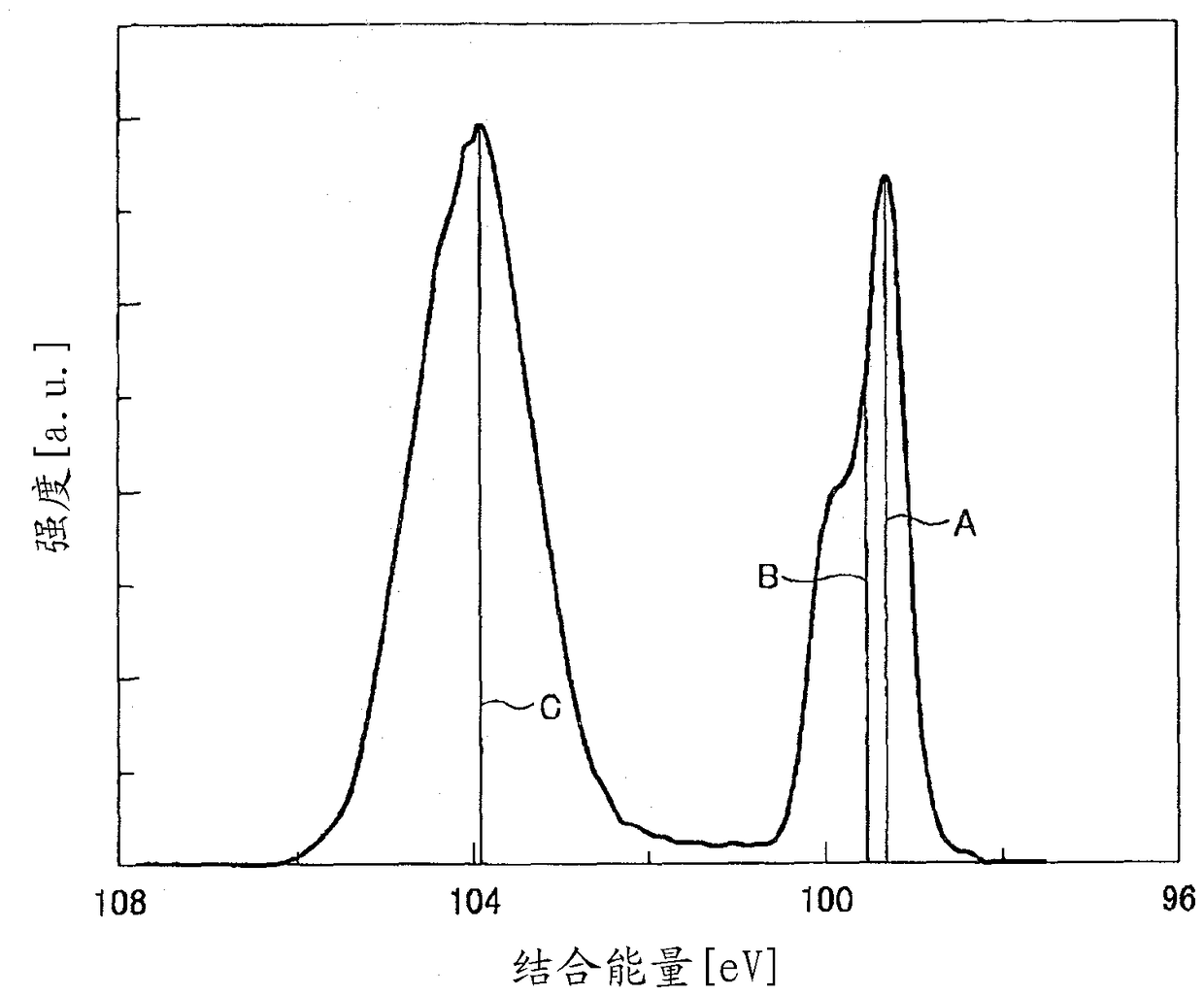
[0081] In addition, in the calculation of the hydrogen termin...

Embodiment 1

[0086] A silicon wafer having a diameter of 300 mm having undergone the rough grinding process was prepared. With respect to the prepared silicon wafer, the conditions were changed as follows, and the finish polishing process was implemented, and then, the cleaning process was implemented with respect to the silicon wafer which completed the finish grinding process.

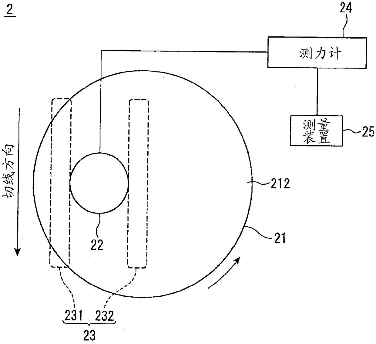
[0087] In the fine grinding process, use image 3 In the grinding device 1 shown, the grinding conditions (the rotation speed of the chassis, the rotation speed of the pressing head, the pressing pressure of the pressing head, etc.) are appropriately adjusted so that the dynamic friction force relative to the wafer is 0.017N / cm 2 . In this finish polishing step, a polishing solution (pH 10.15) in which colloidal silicon was dispersed in an aqueous base solution was used.

[0088] In the cleaning process, the front surface of the silicon wafer is cleaned by supplying a cleaning liquid at a predetermined flow rat...

Embodiment 2

[0099] A silicon wafer having a diameter of 300 mm having undergone the rough grinding process was prepared. With respect to the prepared silicon wafer, the conditions were changed as follows, and the finish polishing process was implemented, and then, the cleaning process was implemented with respect to the silicon wafer which completed the finish grinding process.

[0100] In the fine grinding process, use image 3 In the grinding device 1 shown, the grinding conditions (the rotation speed of the chassis, the rotation speed of the pressing head, the pressing pressure of the pressing head, etc.) are appropriately adjusted so that the dynamic friction force relative to the wafer is 0.017N / cm 2 . In this finish polishing step, a polishing liquid (pH 10.15) in which colloidal silicon was dispersed in an aqueous base solution was used.

[0101] In addition, adjust the grinding conditions appropriately, from 0.014N / cm 2 to 0.021N / cm 2 The dynamic frictional force against the w...


PUM


Abstract

The invention provides a silicon wafer manufacturing method comprising the following procedures of a fine-grinding procedure and a cleaning procedure cleaning the fine-grinded silicon wafer. In the cleaning procedure, at least cleaning liquid containing hydrogen fluoride is employed and controls a cleaning condition in the cleaning procedure and a grinding condition in the fine-grinding procedure to enable wafer front surface hydrogen finality rate to reach more than 87% after the cleaning procedure. Besides, the invention provides a silicon wafer. The silicon wafer is grinded and has front surface haze lower than 20ppb.

Description

technical field [0001] The invention relates to a method for manufacturing a silicon wafer and a silicon wafer. Background technique [0002] In recent years, along with the demand for high integration of semiconductor devices, strict surface characteristics are also required for silicon wafers. [0003] On the other hand, surface roughness having a wavelength of several to several tens of nm, called haze, remains on the front surface of the silicon wafer. When the fog remains on the front side of the silicon wafer, a particle counter that measures the number of particles will recognize the fog as particles. Therefore, there is a need to reduce the haze on the front side of the silicon wafer. [0004] As a solution to the above-mentioned problems, a method for manufacturing a semiconductor wafer is described. The method for manufacturing a semiconductor wafer has rough grinding, fine grinding, and cleaning steps. In the cleaning step, chemical cleaning with an etching amou...

Claims


Application Information

Patent Timeline
Patent Type & Authority Patents(China)
IPC IPC(8): H01L21/02
CPCH01L21/0209H01L21/02096
Inventor 杉森胜久小佐佐和明
Owner SUMCO CORP
Learn More