Self-alignment method for silicon carbide devices

A self-aligned, silicon carbide technology, used in semiconductor devices, semiconductor/solid-state device manufacturing, electrical components, etc., can solve problems such as poor contact, unguaranteed dry etching uniformity, etc., to meet the requirements of reducing uniformity, Avoid the effect of poor contact between the metal electrode and the channel

Active Publication Date: 2015-11-25
GLOBAL POWER TECH CO LTD
View PDF3 Cites 5 Cited by
  • Summary
  • Abstract
  • Description
  • Claims
  • Application Information

AI Technical Summary

Problems solved by technology

[0018] (3) In the above step S5, the uniformity of dry etching cannot be guaranteed, which may easily lead to poor contact between the metal electrode 2 and the channel 1 on the under-etched region of the first dielectric layer 3, and the over-etching of the second dielectric layer 4 The metal electrode 2 on the upper surface of the etched area is in contact with the sidewall of the trench

Method used


Image

  • Self-alignment method for silicon carbide devices
  • Self-alignment method for silicon carbide devices
  • Self-alignment method for silicon carbide devices

Examples


Embodiment 1

[0046] The self-alignment method for silicon carbide devices provided in this embodiment includes the following steps:

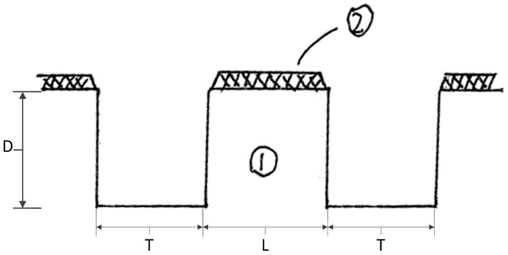
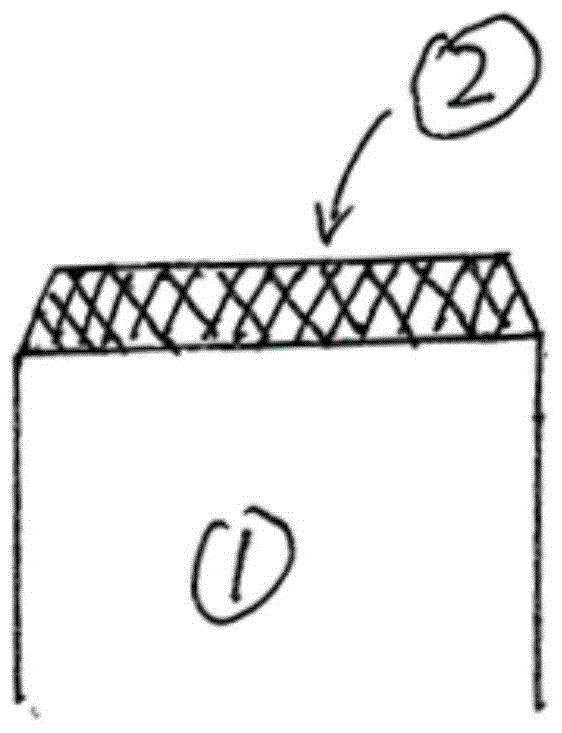
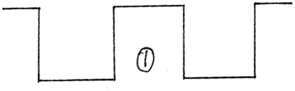
[0047] S1: Prepare exposed channels 1 and grooves on the wafer, as shown in FIG. 4(a);

[0048] S2: Deposit a layer of first dielectric layer 3 on the bottom and side walls of the trench and on the surface of channel 1, and the material of the first dielectric layer 3 contains endpoint detection indicator elements for dry etching, as shown in Figure 4(b) shown; for example, the material of the first dielectric layer 3 is silicon nitride, which contains nitrogen, and the material of the channel 1 and the second dielectric layer 4 does not contain nitrogen, so the material of the first dielectric layer 3 contains Nitrogen is used as an indicator element for endpoint detection of dry etching;

[0049] S3: Deposit a second dielectric layer 4 on the surface of the first dielectric layer 3 to cover the bottom and side walls of the trench and the surface of the ch...

Embodiment 2

[0054] The self-alignment method for silicon carbide devices provided in this embodiment includes the following steps:

[0055] S1: Prepare exposed channels 1 and grooves on the wafer, as shown in FIG. 4(a);

[0056] S2: Deposit a layer of first dielectric layer 3 on the bottom and side walls of the trench and on the surface of channel 1, and the material of the first dielectric layer 3 contains endpoint detection indicator elements for dry etching, as shown in Figure 4(b) shown; for example, the material of the first dielectric layer 3 is silicon nitride, which contains nitrogen, and the material of the channel 1 and the second dielectric layer 4 does not contain nitrogen, so the material of the first dielectric layer 3 contains Nitrogen is used as an indicator element for endpoint detection of dry etching;

[0057] S3: Deposit a second dielectric layer 4 on the surface of the first dielectric layer 3 to cover the bottom and side walls of the trench and the surface of the chan...


PUM


Abstract

The present invention discloses a self-alignment method for silicon carbide devices including the steps as follows: preparing an exposed channel and a groove on a wafer; depositing one layer of first dielectric layer on the bottom and the side wall of the groove and the surface of the channel, wherein, a material of the first dielectric layer contains end point detection indicator elements of a dry etching; depositing one layer of second dielectric layer on the surface of the first dielectric layer so as to cover the bottom and the side wall of the groove and the surface of the channel; coating the surface of the second dielectric layer of the corresponding groove with a photoresistfor filling an interspace of the groove so that the exposed surface of the photoresist aligns at the surface of the second dielectric layer of the corresponding channel; removing the second dielectric layer and the first dielectric layer of the corresponding channel by dry etching so as to expose the surface of the channel; and forming one layer of upper surface metal electrode on the surface of the exposed channel. The self-alignment method can avoid that the second dielectric layer with a bigger thickness deposits on the surface of the first dielectric layer; and the self-alignment method is free from a restriction of special equipment of a chemical machinery lapping method or the dry etching.

Description

technical field [0001] The invention relates to the technical field of processing technology of silicon carbide devices. More specifically, it relates to a self-alignment method for silicon carbide devices. Background technique [0002] As one of the third-generation broadband compound semiconductor materials, silicon carbide has incomparable advantages over traditional silicon and gallium arsenide materials in terms of band gap, maximum field strength, doping concentration, and thermal conductivity, and is especially suitable for high-voltage, High-frequency, high-power, high-irradiation and photoelectric detection technology of certain wavelengths. Therefore, silicon carbide has received extensive attention from researchers in power microwave and optoelectronic devices. [0003] Compared with traditional silicon-based devices, based on the advantages of material properties, silicon carbide devices have the advantages of simple structure, small size and high performance. ...

Claims


Application Information

Patent Timeline
Patent Type & Authority Applications(China)
IPC IPC(8): H01L21/04H01L21/02
CPCH01L21/02H01L21/04H01L29/66053
Inventor 何钧韩超田红林吴海雷梁卫华高怡瑞
Owner GLOBAL POWER TECH CO LTD
Why Eureka
Try Eureka