Packaging structure for FBAR device and manufacturing method thereof

A technology of packaging structure and manufacturing method, which is applied in the direction of semiconductor/solid-state device manufacturing, electric solid-state devices, semiconductor devices, etc., can solve the problems of cumbersome manufacturing process, low production efficiency, long production cycle, etc., and achieve easy popularization and easy mastery , the effect of reducing difficulty

Inactive Publication Date: 2015-11-25
贵州汉天下科技(集团)有限公司
View PDF3 Cites 6 Cited by
  • Summary
  • Abstract
  • Description
  • Claims
  • Application Information

AI Technical Summary

Problems solved by technology

Since this method needs to individually package each chip after dicing, it causes problems such as long production cycle, cumbersome manufacturing process, high production cost and low production efficiency.

Method used


Image

  • Packaging structure for FBAR device and manufacturing method thereof
  • Packaging structure for FBAR device and manufacturing method thereof
  • Packaging structure for FBAR device and manufacturing method thereof

Examples


Embodiment Construction

[0053] In order to better understand and illustrate the present invention, the present invention will be further described in detail below in conjunction with the accompanying drawings.

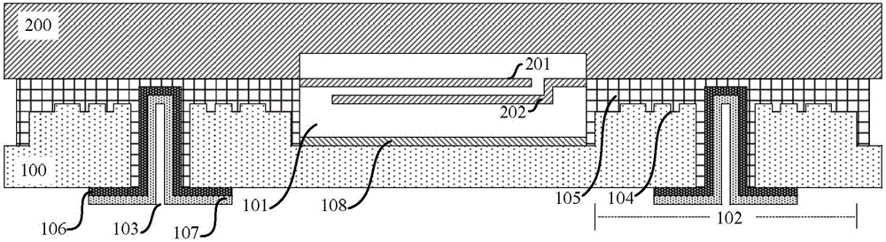
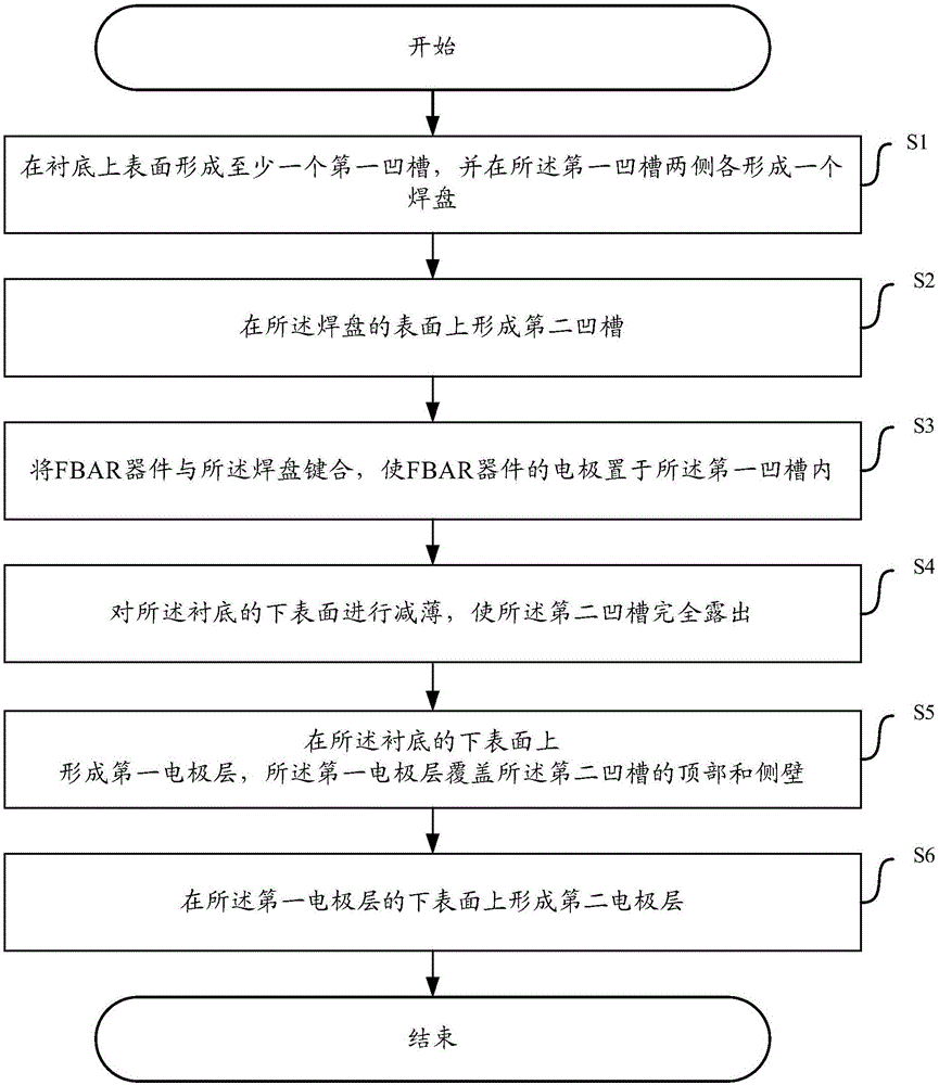
[0054] The invention provides an FBAR device packaging structure. Please refer to figure 1 ,figure 1 It is a schematic diagram of the packaging structure of an FBAR device provided according to the present invention. As shown in the figure, the package structure includes:

[0055] Substrate 100, at least one first groove 101, pad 102, second groove 103, first electrode layer 106, second electrode layer 107 and at least one FBAR device 200;

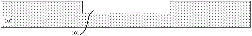
[0056] At least one first groove 101 is formed on the upper surface of the substrate 100;

[0057] A welding pad 102 is formed on both sides of the first groove 101;

[0058] The second groove 103 is formed on the surface of the pad 102;

[0059] The FBAR device 200 is bonded to the pad 102, and the electrodes of the FBAR device 200 are placed in the...


PUM


Abstract

The invention provides a packaging structure for an FBAR device. The packaging structure comprises a substrate, at least one first groove, bonding pads, second grooves, a first electrode layer, a second electrode layer and at least one FBAR device plate, wherein the at least one first groove is formed in the upper surface of the substrate; one bonding pad is formed on two sides of the first groove respectively; each second groove is formed in the surface of the corresponding bonding pad; the FBAR device is bonded with the bonding pads, and the electrodes of the FBAR device are arranged in the first groove; the first electrode layer is formed on the lower surface of the substrate, and overlays the tops and the side walls of the second grooves at the same time; and the second electrode layer is formed on the lower surface of the first electrode layer. Correspondingly, the invention also discloses a manufacturing method of the packaging structure for the FBAR device. Through the implementation of the packaging structure for the FBAR device and the manufacturing method of the packaging structure for the FBAR device, the difficulty of the packaging technology can be reduced, and the production technology and production cycle are optimized, so that the packaging cost is greatly reduced.

Description

technical field [0001] The invention relates to the technical field of semiconductor device packaging and manufacturing, in particular to an FBAR device packaging structure and a manufacturing method thereof. Background technique [0002] With the development of thin film and micro-nano manufacturing technology, electronic devices are developing rapidly in the direction of miniaturization, high-density multiplexing, high frequency and low power consumption. The film bulk acoustic resonator (FBAR) developed in recent years adopts an advanced resonance technology, which converts electrical energy into sound waves through the inverse piezoelectric effect of piezoelectric films to form resonance. This resonance technology can be used to make Advanced components such as thin-film frequency shaping devices. FBAR devices have many advantages such as small size, high operating frequency, high efficiency, low insertion loss, large out-of-band suppression, high power capacity, low te...

Claims


Application Information

Patent Timeline
Patent Type & Authority Applications(China)
IPC IPC(8): H01L23/02H01L23/48H01L21/50
Inventor 杨清华欧毅刘杰赖亚明吴光胜顾程先陈庆朱丽娜
Owner 贵州汉天下科技(集团)有限公司
Why Eureka
Try Eureka