Chip wire welding jig, leading-out method for chip lead and chip product

A chip and jig technology, applied in the direction of electrical components, electrical solid devices, circuits, etc., can solve the problems of inability to carry out continuous operation, inability to pull off, etc., and achieve the effects of adjustable position, reduction of substrates, and simple processing process

Active Publication Date: 2015-11-25
GALAXYCORE SHANGHAI
View PDF4 Cites 0 Cited by
  • Summary
  • Abstract
  • Description
  • Claims
  • Application Information

AI Technical Summary

Problems solved by technology

The requirement of this existing technology is that both the first soldering point 6 and the second soldering point 7 need to be reliably welded,

Method used


Image

  • Chip wire welding jig, leading-out method for chip lead and chip product
  • Chip wire welding jig, leading-out method for chip lead and chip product
  • Chip wire welding jig, leading-out method for chip lead and chip product

Examples


Example Embodiment

[0045] The specific implementation of the chip bonding wire fixture, the chip lead extraction method and the finished chip of the present invention will be described in detail below in conjunction with the accompanying drawings.
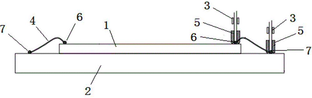
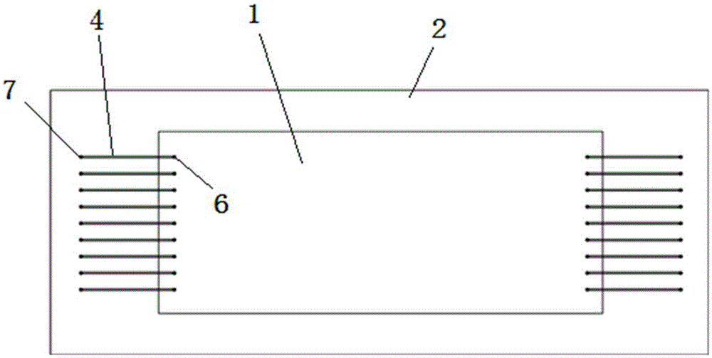
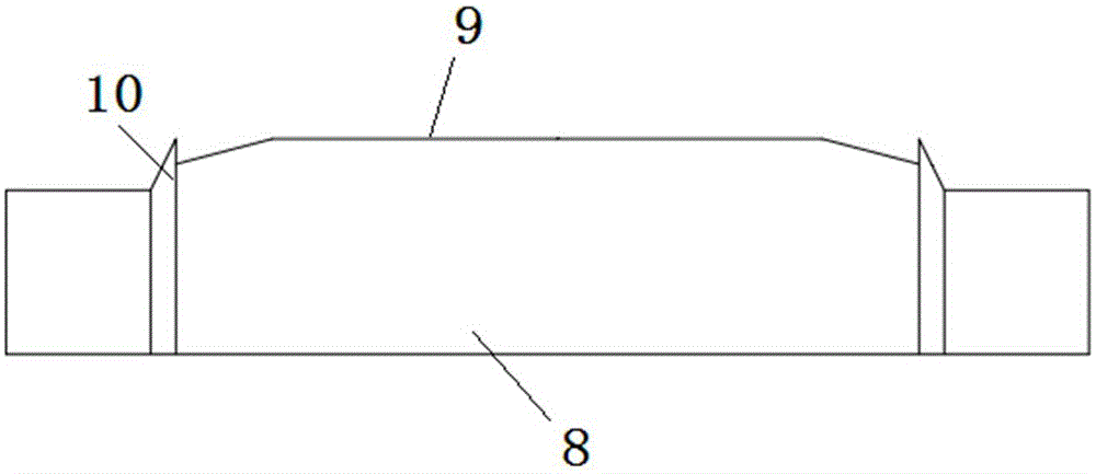
[0046] See attached image 3 , The chip bonding wire fixture 8 has a square structure, and its shape can be adjusted according to the batch of chips. A chip platform 9 is set in the middle of the fixture, and blades 10 are set on the left and right sides of the chip platform 9, and the blades of the blades protrude from the chip platform. 9. The shape of the chip platform 9 is determined according to the shape of the chip. The end of the chip platform close to the blade 10 is inclined toward the blade, and the height of the blade portion of the blade is not higher than the upper surface of the chip.

[0047] For chips with wires on both sides, blades are set on both sides of the chip platform 9 to perform wire bonding. For chips with four-side wires, bla...


PUM


Abstract

The invention relates to the technical field of manufacturing of integrated circuit chips, and discloses a chip wire welding jig. The chip wire welding jig comprises a chip platform in the middle, blades are arranged on the left and right sides of the chip platform, and the cutting edges of the blades protrude the chip platform. The invention further discloses a leading-out method for a chip lead realized by using the chip wire welding jig and a chip product produced by the method. The lead can be led out from the chip by single welding, so the processing process is simple. The leading-out direction of the lead can be adjusted, so the lead is suitable for design of various different circuit boards. The jig is simple in structure and adjustable in blade position, and is suitable for processing various leads and chips with various sizes.

Description

technical field [0001] The invention relates to the technical field of integrated circuit chip manufacturing and processing, in particular to a chip bonding wire jig, a chip lead-out method and a chip finished product. Background technique [0002] The chip bonding process is applied to the integrated circuit packaging process, and its purpose is to lead out the electrical connection points of the integrated circuit chip with leads to form integrated circuit pins. [0003] See attached figure 1 , 2 , the traditional chip bonding process is to first place the chip 1 on the substrate 2, fix the lead 4 through the wire clip 3, firstly weld the first solder spot 6 on the chip 1 through the chopper 5, and then connect the lead 4 Pull it to the substrate 2, and weld the second solder spot 7 on the substrate 2. After the second solder spot 7 is welded, the chopper 5 is lifted upwards. The lead wire 4 is torn off, and the welding of one lead wire is completed. The wire bonding o...

Claims


Application Information

Patent Timeline
IPC IPC(8): H01L23/48H01L21/60
CPCH01L2224/48091H01L2224/49175H01L2224/78301H01L2224/85181H01L2924/00014
Inventor 蒋永新王军平朱玉萍
Owner GALAXYCORE SHANGHAI
Why Eureka
Try Eureka