Preparation method of N-type silicon chip a-Si:H film for heterojunction with intrinsic thin layer (HIT) battery

An a-si, N-type technology, used in circuits, photovoltaic power generation, electrical components, etc., can solve the problems of lack of preparation technology, difficult to meet the quality of thin films, etc., and achieve the effect of improving efficiency

Inactive Publication Date: 2015-11-25
48TH RES INST OF CHINA ELECTRONICS TECH GROUP CORP
View PDF2 Cites 4 Cited by
  • Summary
  • Abstract
  • Description
  • Claims
  • Application Information

AI Technical Summary

Problems solved by technology

At present, the preparation technology of N-type silicon wafer a-Si:H film for HIT battery is relatively lacking, and the existing amorphous silicon film deposition is mainly used for amorphous silicon battery, and the film quality is difficult to meet the requirements of HIT battery

Method used


Image

  • Preparation method of N-type silicon chip a-Si:H film for heterojunction with intrinsic thin layer (HIT) battery

Examples


Embodiment 1

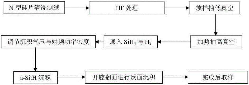
[0025] A kind of preparation method of N-type silicon chip a-Si:H film for HIT battery of the present invention, technological process is as figure 1 shown, including the following steps:

[0026] (1) N-type silicon wafer cleaning and texturing: N-type silicon wafers used for HIT cells are cleaned and textured, mainly to complete the removal of the mechanical damage layer on the surface of the silicon wafer and the preparation of the pyramid texture, and remove the damaged layer on the surface of the silicon wafer on one side 18μm, the diagonal size of the pyramid is 5-8μm.

[0027] (2) Deoxidation layer treatment (HF treatment): After the N-type silicon wafer is cleaned and textured, it is placed in an HF solution with a volume concentration of 2.5% and reacted for 16 seconds to mainly remove the natural oxide layer on the surface of the silicon wafer, and the process is completed. Take it out and rinse it with deionized water, N 2 blow dry.

[0028] (3) Deposition of a-Si...

Embodiment 2

[0036] A kind of preparation method of N-type silicon chip a-Si:H film for HIT battery of the present invention, technological process is as figure 1 shown, including the following steps:

[0037] (1) N-type silicon wafer cleaning and texturing: N-type silicon wafers used for HIT cells are cleaned and textured, mainly to complete the removal of the mechanical damage layer on the surface of the silicon wafer and the preparation of the pyramid texture, and remove the damaged layer on the surface of the silicon wafer on one side 22μm, the diagonal size of the pyramid is 6-10μm.

[0038] (2) Deoxidation layer treatment (HF treatment): After the N-type silicon wafer is cleaned and textured, it is placed in an HF solution with a volume concentration of 3%, and reacted for 10s to mainly remove the natural oxide layer on the surface of the silicon wafer, and the process is completed. Take it out and rinse it with deionized water, N 2 blow dry.

[0039] (3) Deposition of a-Si:H thin f...


PUM

PropertyMeasurementUnit
sizeaaaaaaaaaa
thicknessaaaaaaaaaa

Abstract

The invention discloses a preparation method of an N-type silicon chip a-Si:H film for a heterojunction with intrinsic thin layer (HIT) battery. The preparation method comprises the following steps: (1) cleaning and texturing an N-type silicon chip; (2) carrying out oxidation layer removal treatment; (3) putting the N-type silicon chip into a plasma enhanced chemical vapor deposition (PECVD) cavity, firstly extracting background vacuum, heating and warming the N-type silicon chip, extracting high vacuum, introducing deposition gases SiH4 and H2, carrying out a-Si:H film deposition on the front surface of the N-type silicon chip, and turning over the silicon chip; and (4) repeating the processes in the step (3), carrying out a-Si:H film deposition on the back surface of the N-type silicon chip, and finishing preparation of the N-type silicon chip a-Si:H film for the HIT battery. According to the preparation method, the a-Si:H film with high passivation quality and low defect density can be obtained; the surface quality of the silicon chip is greatly improved; and the efficiency of the HIT battery is effectively improved.

Description

technical field [0001] The invention relates to a preparation method of an N-type silicon wafer a-Si:H thin film for HIT batteries, in particular to a preparation method of an N-type silicon wafer a-Si:H thin film for HIT batteries with high passivation quality and low defect density. Background technique [0002] As a kind of high-efficiency battery, HIT solar cell not only utilizes the low-temperature thin film deposition process, but also takes advantage of the high mobility of crystalline silicon, and the preparation process is simple. Among them, the crystalline silicon part of the HIT battery is generally an N-type silicon wafer, which has the characteristics of high open circuit voltage and high conversion efficiency. On the one hand, HIT cells are completely different from traditional crystalline silicon solar cells in terms of structure and manufacturing process, and the existing process is basically inapplicable to HIT cells; but on the other hand, it can guarantee...

Claims


Application Information

Patent Timeline
Patent Type & Authority Applications(China)
IPC IPC(8): H01L31/18H01L31/0747
CPCH01L31/0747H01L31/1804Y02E10/50Y02P70/50
Inventor 汪已琳曹骞杨晓生彭卓寅
Owner 48TH RES INST OF CHINA ELECTRONICS TECH GROUP CORP
Why Eureka
Try Eureka